×
Request Free Sample ×

Kindly complete the form below to receive a free sample of this Report

* Please use a valid business email

Leading companies partner with us for data-driven Insights

clients tt-cursor
Hero Background
English
Chinese
French
Japanese
Korean
German
Spanish

High Density Interconnect PCB Market Size

ID: MRFR/SEM/5821-CR
100 Pages
Aarti Dhapte
April 2023

High Density Interconnect PCB Market Size, Share and Research Report By Interconnection Layers (1 Layer (1+N+1) HDI, 2 or more layers (2+N+2) HDI, and All Layers HDI), Application (into Consumer Electronics, Automotive, Military and Defense, Healthcare, Industrial/ Manufacturing, and Others), and By Region (North America, Europe, Asia-Pacific, Middle East & Africa, and South America) - Industry Forecast Till 2035

Share:
Download PDF ×

We do not share your information with anyone. However, we may send you emails based on your report interest from time to time. You may contact us at any time to opt-out.

High Density Interconnect PCB Market Infographic
×
High Density Interconnect PCB Market Infographic Full View
Purchase Options

High Density Interconnect Pcb Size

High Density Interconnect PCB Market Growth Projections and Opportunities

In the realm of electronics, high-density interconnect (HDI) printed circuit boards (PCBs) have emerged as a transformative technology, revolutionizing the design and manufacturing of electronic devices. HDI PCBs are characterized by their intricate microvias, blind vias, and via-in-pad (VIP) structures, enabling them to pack significantly more circuitry into a smaller space compared to traditional PCBs. This remarkable capability has propelled HDI PCBs to the forefront of modern electronics, catering to the ever-increasing demand for miniaturization and enhanced performance.

The genesis of HDI PCB technology can be traced back to the 1980s, when the pursuit of smaller and more powerful electronic devices fueled the need for more efficient packaging solutions. Conventional PCBs, with their larger vias and limited routing capabilities, were no longer sufficient to accommodate the demands of shrinking components and complex circuitry. HDI PCBs emerged as the answer, offering a quantum leap in circuit density and paving the way for a new era of electronic innovation.

At the heart of HDI PCB technology lies the concept of microvias, which are tiny vias measuring just a few micrometers in diameter. These microvias enable designers to connect different layers of the circuit board with much finer lines and tighter spacing, dramatically increasing the available circuit density. Blind vias, which are buried within the PCB layers, further enhance routing flexibility and contribute to the overall compactness of the circuit board.

The introduction of VIP technology in the early 2000s marked a significant milestone in HDI PCB development. VIP structures place vias directly within the solder pads of components, eliminating the need for separate via holes and further reducing the space occupied by circuitry. This innovation has been instrumental in enabling the realization of ultra-miniature electronic devices, such as smartphones and wearable electronics.

The advantages of HDI PCBs extend far beyond their remarkable size reduction capabilities. They offer a multitude of benefits that make them indispensable in today's demanding electronics landscape:

Enhanced Performance: HDI PCBs support higher signal speeds and frequencies, enabling faster data transmission and improved overall system performance. This is crucial for applications such as high-speed data communication, wireless networking, and advanced computing.

Reduced Power Consumption: The smaller components and shorter lines in HDI PCBs contribute to lower power consumption, making them an ideal choice for energy-efficient electronic devices.

Improved Reliability: HDI PCBs are less susceptible to noise and interference, leading to enhanced system reliability and reduced susceptibility to malfunctions.

Greater Flexibility: HDI PCBs can be designed in a wider range of shapes and sizes, providing greater flexibility for engineers and designers to create innovative form factors.

The demand for HDI PCB manufacturing is soaring driven by the relentless pursuit of miniaturization, performance enhancement, and energy efficiency in electronic devices. This growth is further fueled by the expansion of applications that demand high-density circuitry, such as smartphones, tablets, wearable electronics, and high-performance computing systems.

As the demand for HDI PCBs continues to rise, manufacturers are constantly innovating to develop new techniques and processes that further enhance the capabilities of these remarkable circuit boards. These advancements include the use of laser drilling for precise via formation, the development of advanced materials with superior electrical and thermal properties, and the implementation of sophisticated design tools that optimize circuit placement and routing.

The future of HDI PCB technology is bright, with continued advancements promising even smaller, faster, and more powerful circuit boards. As we move into the era of the Internet of Things (IoT) and artificial intelligence (AI), HDI PCBs will play a pivotal role in enabling the development of increasingly complex and interconnected devices that will shape the future of technology.
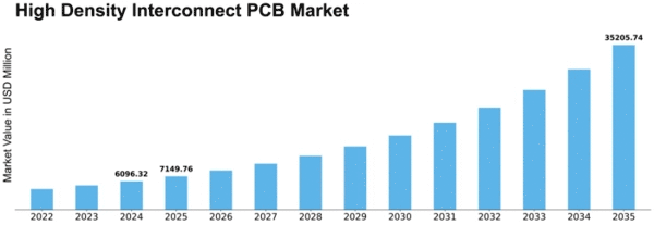
High Density Interconnect PCB Market Size Graph
Author
Aarti Dhapte
Team Lead - Research

She holds an experience of about 6+ years in Market Research and Business Consulting, working under the spectrum of Information Communication Technology, Telecommunications and Semiconductor domains. Aarti conceptualizes and implements a scalable business strategy and provides strategic leadership to the clients. Her expertise lies in market estimation, competitive intelligence, pipeline analysis, customer assessment, etc.

Leave a Comment

FAQs

What is the market size for 2035, for the High Density Interconnect PCB Market?

High Density Interconnect PCB Market is Projected to Reach USD 35205.74 billion by 2035

What is the growth rate of the High Density Interconnect PCB market?

The global market is projected to grow at a CAGR of 17.28% during the forecast period, 2025 to 2035.

Which region held the largest market share in the High Density Interconnect PCB market?

From 2024 to 2032, Asia Pacific has the potential to achieve the top position in the global market.

Who are the prominent players in the High Density Interconnect PCB market?

Unimicron, Epec, LLC, TTM Technologies Inc., RayMing Technology, HiTech Circuits, NCAB Group Corporation, Millennium Circuits Limited, Tripod Technology, Zhen Ding Tech. Group Technology Holding Limited, AKM Meadville, Meiko Electronics Co., Ltd., Sierra Circuits Inc., Compeq Manufacturing Co., Ltd, AT & S (Austria Technologie & Systemtechnik Aktiengesellschaft), Advanced Circuits, and DAP Coroporation.

Market Summary

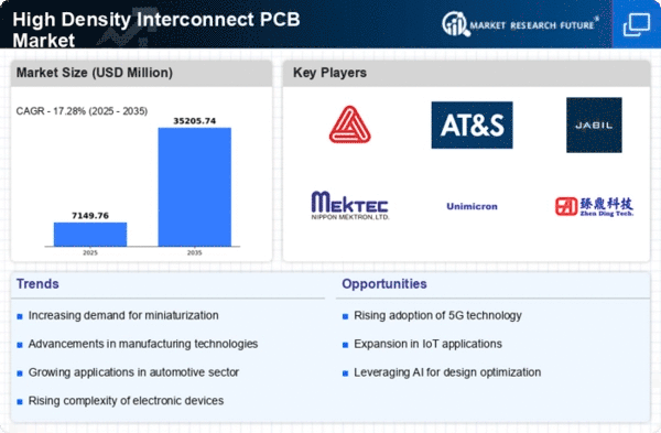
As per MRFR analysis, the High Density Interconnect PCB Market Size was estimated at 6096.32 USD Million in 2024. The High Density Interconnect PCB industry is projected to grow from 7149.88 USD Million in 2025 to 35205.74 USD Million by 2035, exhibiting a compound annual growth rate (CAGR) of 17.28 during the forecast period 2025 - 2035.

Key Market Trends & Highlights

The High Density Interconnect PCB Market is poised for robust growth driven by technological advancements and increasing demand across various sectors.

  • The market is experiencing a notable trend towards the miniaturization of electronics, particularly in North America. Adoption of advanced materials is becoming increasingly prevalent, especially in the Asia-Pacific region. Sustainability initiatives are gaining traction, influencing design and manufacturing processes across multiple segments. The rising demand for consumer electronics and advancements in telecommunications are key drivers propelling market expansion.

Market Size & Forecast

2024 Market Size 6096.32 (USD Million)
2035 Market Size 35205.74 (USD Million)
CAGR (2025 - 2035) 17.28%
Largest Regional Market Share in 2024 North America

Major Players

<p>Avery Dennison (US), AT&amp;S (AT), Jabil (US), Nippon Mektron (JP), Unimicron Technology (TW), Zhen Ding Technology Holding Limited (TW), Shenzhen Fastprint Circuit Tech (CN), Samsung Electro-Mechanics (KR), Flex Ltd. (SG)</p>

Market Trends

The High Density Interconnect PCB Market is currently experiencing a transformative phase, driven by the increasing demand for compact and efficient electronic devices. As technology advances, manufacturers are compelled to innovate, leading to the development of PCBs that can accommodate higher circuit densities. This trend is particularly evident in sectors such as telecommunications, automotive, and consumer electronics, where the need for miniaturization and enhanced performance is paramount. Furthermore, the integration of advanced materials and manufacturing techniques is reshaping the landscape, allowing for greater functionality within smaller footprints. In addition, sustainability considerations are becoming more prominent within the High Density Interconnect PCB Market. Companies are increasingly focusing on eco-friendly materials and processes, responding to both regulatory pressures and consumer preferences for greener products. This shift not only aligns with global sustainability goals but also opens new avenues for innovation. As the market evolves, it appears poised for continued growth, with emerging technologies and changing consumer demands likely to shape its trajectory in the coming years.

Miniaturization of Electronics

The trend towards miniaturization is profoundly influencing the High Density Interconnect PCB Market. As devices become smaller, the need for PCBs that can support higher component densities is critical. This shift is particularly relevant in sectors such as mobile devices and wearables, where space constraints necessitate innovative design solutions.

Adoption of Advanced Materials

The use of advanced materials in PCB manufacturing is gaining traction within the High Density Interconnect PCB Market. Materials that offer improved thermal management and electrical performance are increasingly favored, enabling manufacturers to create more efficient and reliable products. This trend reflects a broader movement towards enhancing the overall performance of electronic devices.

Sustainability Initiatives

Sustainability is emerging as a key focus in the High Density Interconnect PCB Market. Manufacturers are exploring eco-friendly materials and processes to reduce environmental impact. This trend not only meets regulatory requirements but also caters to a growing consumer demand for sustainable electronics, potentially reshaping industry practices.

High Density Interconnect PCB Market Market Drivers

Market Growth Projections

The Global High Density Interconnect PCB Market Industry is poised for remarkable growth, with projections indicating a rise from 6.1 USD Billion in 2024 to an impressive 35.2 USD Billion by 2035. This trajectory reflects the increasing reliance on high-density interconnect technologies across various sectors, including telecommunications, automotive, and consumer electronics. The anticipated compound annual growth rate of 17.28% from 2025 to 2035 underscores the industry's potential for expansion. As businesses and consumers alike seek more efficient and compact electronic solutions, the demand for high-density interconnect PCBs is likely to escalate, driving innovation and investment in this critical sector.

Advancements in Technology

Technological advancements play a crucial role in shaping the Global High Density Interconnect PCB Market Industry. Innovations in materials, such as high-frequency laminates and advanced substrate technologies, enable the production of PCBs that support faster signal transmission and improved thermal management. These advancements are particularly relevant in sectors like automotive and aerospace, where reliability and performance are critical. As the industry evolves, the integration of smart technologies and IoT devices further propels the demand for high-density interconnect solutions. The market is expected to witness a compound annual growth rate of 17.28% from 2025 to 2035, indicating a robust trajectory driven by these technological enhancements.

Surge in Consumer Electronics

The consumer electronics sector is a primary driver of the Global High Density Interconnect PCB Market Industry, as the proliferation of smart devices continues unabated. Products such as tablets, wearables, and smart home devices necessitate PCBs that can deliver high performance in compact designs. This demand is reflected in the market's anticipated growth, with a valuation of 6.1 USD Billion expected in 2024. The trend towards smart technology adoption, coupled with consumer preferences for multifunctional devices, propels manufacturers to innovate and enhance PCB capabilities. As a result, the industry is likely to see sustained growth as it adapts to the evolving landscape of consumer electronics.

Growth in Automotive Electronics

The automotive sector significantly influences the Global High Density Interconnect PCB Market Industry, driven by the increasing complexity of electronic systems in vehicles. Modern automobiles incorporate advanced driver-assistance systems, infotainment, and connectivity features, all of which require sophisticated PCB solutions. As electric vehicles gain traction, the demand for high-density interconnect PCBs is expected to rise, given their ability to support the intricate electronic architectures of these vehicles. The market's expansion is further underscored by projections indicating a growth to 35.2 USD Billion by 2035, highlighting the automotive industry's pivotal role in shaping future PCB requirements.

Rising Demand for Miniaturization

The Global High Density Interconnect PCB Market Industry experiences a notable surge in demand for miniaturization across various sectors, particularly in consumer electronics and telecommunications. As devices become increasingly compact, the need for PCBs that can accommodate higher component densities without compromising performance becomes paramount. This trend is exemplified by the smartphone industry, where manufacturers continuously strive to integrate more features into smaller form factors. The market is projected to reach 6.1 USD Billion in 2024, reflecting the industry's adaptation to these evolving consumer preferences. The push for miniaturization is likely to drive innovation in PCB design and manufacturing processes.

Emerging Markets and Global Expansion

Emerging markets present substantial opportunities for the Global High Density Interconnect PCB Market Industry, as economic development fosters increased demand for electronic products. Countries in Asia-Pacific and Latin America are witnessing rapid urbanization and rising disposable incomes, leading to greater consumption of consumer electronics and automotive technologies. This trend is likely to drive the need for high-density interconnect solutions, as manufacturers seek to establish a foothold in these burgeoning markets. The anticipated growth trajectory, with a CAGR of 17.28% from 2025 to 2035, suggests that the industry will continue to expand its global presence, adapting to the unique demands of diverse markets.

Market Segment Insights

By Application: Consumer Electronics (Largest) vs. Telecommunications (Fastest-Growing)

<p>In the High Density Interconnect PCB Market, the<a href="https://www.marketresearchfuture.com/reports/consumer-electronics-mlcc-market-35506"> Consumer Electronics</a> sector holds the largest market share, largely driven by the ever-increasing demand for electronic devices such as smartphones, tablets, and laptops. This sector continues to dominate due to the constant innovation and reduced size of circuits that High Density Interconnects provide. Conversely, the Telecommunications sector is rapidly gaining traction, reflecting significant investment in infrastructure upgrades and advanced communication technologies, thus positioning itself as the fastest-growing segment. As technology evolves, the growth of both sectors is propelled by the increasing need for enhanced performance, connectivity, and miniaturization. The rise of the Internet of Things (IoT) further boosts the demand for High Density Interconnect PCBs in both Consumer Electronics and Telecommunications, as these applications require high-performance interconnects to support varied functionalities. These sectors are expected to continue expanding as innovations and consumer demands escalate.</p>

<p>Telecommunications: Dominant vs. Automotive: Emerging</p>

<p>The Telecommunications sector stands as a dominant force in the High Density Interconnect PCB Market due to its critical role in facilitating advanced communication and networking technologies. This sector benefits from the increasing demand for high-speed data transmission and connectivity, spurred by the deployment of 5G networks and the rise of smart devices. On the other hand, the Automotive sector is an emerging player in this market, fueled by the growing integration of electronic components in vehicles, including advanced driver-assistance systems (ADAS) and infotainment systems. As the automotive industry shifts towards electric and automated vehicles, the need for sophisticated PCBs is anticipated to surge, creating new opportunities for growth and innovation.</p>

By End Use: Industrial (Largest) vs. Healthcare (Fastest-Growing)

<p>The High Density Interconnect (HDI) PCB Market showcases a diverse array of end uses, with the industrial segment commanding the largest market share. This sector encompasses a wide range of applications, from manufacturing machinery to automation systems, benefitting from the intricate designs and enhanced performance capabilities of HDI technology. Close behind, healthcare applications are rapidly growing, driven by the increasing demand for advanced medical devices and diagnostic equipment that utilize HDI PCBs for their compact and efficient circuitry.</p>

<p>Healthcare: Healthcare (Emerging) vs. Industrial (Dominant)</p>

<p>The healthcare segment is emerging as a significant user of High Density Interconnect PCBs, owing to the rising trend of miniaturization in medical devices and increased deployment of telemedicine technologies. HDI PCBs allow for more functionality in smaller spaces, which is critical in devices such as wearable health monitors and diagnostic equipment. Conversely, the industrial segment remains dominant, leveraging HDI technology for high-performance applications in automation, control systems, and various industrial equipment. Both segments are essential to the market, yet their characteristics and growth trajectories differ markedly, highlighting diverse opportunities in the HDI PCB landscape.</p>

By Material Type: Copper (Largest) vs. Polyimide (Fastest-Growing)

<p>The High Density Interconnect PCB Market exhibits a diverse material type distribution. Copper stands out as the largest segment, owing to its excellent electrical conductivity and thermal properties, which make it a preferred choice for high-performance applications. Following copper, materials like Aluminum and FR-4 hold notable shares, while emerging materials such as Polyimide and Ceramic are gaining traction in specialized segments. The demand for high-density interconnects drives the need for reliable materials that can meet performance requirements without compromising on efficiency. Growth trends in this segment are primarily influenced by technological advancements and the demand for lightweight, flexible, and durable solutions. Polyimide is recognized as the fastest-growing material type, largely due to its resistance to high temperatures and flexibility, which align well with the increasing complexity of electronic devices. As industries push for miniaturized designs, the role of innovative materials becomes more crucial in enhancing device performance, longevity, and reducing overall weight.</p>

<p>Copper (Dominant) vs. Ceramic (Emerging)</p>

<p>Copper holds a dominant position in the High Density Interconnect PCB Market, largely due to its superior conductivity and thermal performance, making it ideal for high-frequency applications. Its electroplated versions are widely used to create intricate circuit designs while ensuring reliability in electronics. In contrast, Ceramic, categorized as an emerging material, is drawing interest due to its unique properties such as low dielectric loss and high thermal stability. While Copper is favored for its cost-effectiveness, Ceramic offers advantages in high-frequency and high-temperature environments. As the market moves towards more advanced applications, including RF and microwave technologies, the shift towards Ceramic is anticipated to grow, appealing to sectors that prioritize performance over costs.</p>

By Layer Count: Multi-Layer (Largest) vs. High Layer Count (Fastest-Growing)

<p>In the High Density Interconnect PCB Market, the market share distribution reveals that Multi-Layer PCBs dominate the segment, with widespread adoption in various electronics due to their advanced capabilities. It is followed by Double Layer PCBs, which offer a balanced performance-to-cost ratio, making them a preferred choice for many applications. Single Layer PCBs, while essential for basic circuitry, occupy a smaller share due to limited functionality, leaving Flexible PCBs and High Layer Count variants to fill specialized niches in the industry.</p>

<p>Multi-Layer (Dominant) vs. High Layer Count (Emerging)</p>

<p>Multi-Layer PCBs, being the cornerstone of the High Density Interconnect PCB Market, are characterized by their ability to incorporate multiple layers of circuitry, which allows for greater functionality and miniaturization in electronic devices. This segment thrives in high-performance applications such as computers and telecommunications, where space is at a premium. In contrast, High Layer Count PCBs are emerging as a strong competitor, catering to niche applications that require extremely complex routing and high connection density. This segment is driven by innovations in technology and the increasing demand for more sophisticated electronic systems, positioning High Layer Count PCBs as critical players in the growing market.</p>

By Manufacturing Technology: Printed Circuit Board (Largest) vs. Embedded Technology (Fastest-Growing)

<p>In the High Density Interconnect PCB Market, Printed Circuit Board technology holds the largest share, significantly influencing the overall dynamics of this segment. This dominance is attributed to its broad applicability across various sectors, including consumer electronics and telecommunications, ensuring its continued relevance in the market landscape. Conversely, Embedded Technology is emerging as the fastest-growing segment, driven by the increasing demand for miniaturization in electronic devices. As industries prioritize compact designs and enhanced functionality, embedded designs within PCBs are gaining traction, leading to significant growth opportunities in this area. The rise of IoT and smart devices further propels this segment, marking a transformative shift in manufacturing preferences.</p>

<p>Embedded Technology (Dominant) vs. Hybrid Technology (Emerging)</p>

<p>Embedded Technology is notable for its integration capabilities, enabling advanced functionalities within compact designs. This segment has become a critical part of the High Density Interconnect PCB Market as it facilitates the development of more sophisticated electronic devices with enhanced performance and reduced space requirements. Conversely, Hybrid Technology is emerging as a significant contender by combining various manufacturing techniques to optimize PCB production. While still gaining ground, it offers unique advantages in flexibility and customization, appealing to niche markets that require tailored solutions for high-performance applications. As both segments evolve, they represent different strategies within the manufacturing landscape, reflecting the industry's shift towards innovation and efficiency.</p>

Get more detailed insights about High Density Interconnect PCB Market Research Report – Forecast 2035

Regional Insights

North America : Market Leader in Innovation

North America is poised to maintain its leadership in the High Density Interconnect PCB market, holding a significant market share of $3040.0M in 2024. The region's growth is driven by robust demand from sectors such as telecommunications, automotive, and consumer electronics. Regulatory support for advanced manufacturing technologies further catalyzes this growth, ensuring compliance with environmental standards and promoting innovation. The competitive landscape is characterized by key players like Avery Dennison and Jabil, who are investing heavily in R&D to enhance product offerings. The U.S. and Canada are the leading countries, with a strong focus on technological advancements and sustainability. This region's commitment to high-quality manufacturing and innovation positions it as a global hub for PCB production.

Europe : Emerging Market with Potential

Europe's High Density Interconnect PCB market is projected to grow, with a market size of $1820.0M. The region benefits from increasing demand in sectors such as automotive and industrial electronics, driven by the push for miniaturization and efficiency. Regulatory frameworks, including the EU's RoHS directive, are shaping the market by promoting environmentally friendly manufacturing practices, which are essential for compliance and market acceptance. Leading countries like Germany and France are at the forefront, hosting major players such as AT&S and Flex Ltd. The competitive landscape is evolving, with a focus on innovation and sustainability. European manufacturers are increasingly collaborating with tech firms to develop advanced PCB solutions, ensuring they remain competitive in a rapidly changing market.

Asia-Pacific : Rapid Growth and Expansion

The Asia-Pacific region is witnessing rapid growth in the High Density Interconnect PCB market, with a market size of $1500.0M. This growth is fueled by the increasing demand for consumer electronics and automotive applications, particularly in countries like China, Japan, and South Korea. The region's favorable manufacturing environment, coupled with government initiatives to support technology advancements, is driving market expansion. China stands out as a manufacturing hub, hosting key players like Nippon Mektron and Zhen Ding Technology Holding Limited. The competitive landscape is marked by aggressive pricing strategies and innovation, as companies strive to meet the growing demand for high-performance PCBs. The region's focus on enhancing production capabilities positions it as a critical player in The High Density Interconnect PCB.

Middle East and Africa : Emerging Market Opportunities

The Middle East and Africa region is gradually emerging in the High Density Interconnect PCB market, with a market size of $736.32M. The growth is driven by increasing investments in technology and infrastructure, particularly in sectors like telecommunications and automotive. Regulatory initiatives aimed at enhancing manufacturing standards are also contributing to market development, fostering a conducive environment for PCB production. Countries like South Africa and the UAE are leading the charge, with a growing number of local manufacturers entering the market. The competitive landscape is characterized by a mix of established players and new entrants, focusing on innovation and quality. As the region continues to develop its technological capabilities, it presents significant opportunities for growth in the PCB sector.

Key Players and Competitive Insights

The High Density Interconnect PCB Market is characterized by a dynamic competitive landscape, driven by technological advancements and increasing demand for miniaturized electronic devices. Key players such as Jabil (US), AT&S (AT), and Samsung Electro-Mechanics (KR) are at the forefront, each adopting distinct strategies to enhance their market positioning. Jabil (US) focuses on innovation and digital transformation, leveraging advanced manufacturing technologies to optimize production efficiency. Meanwhile, AT&S (AT) emphasizes regional expansion, particularly in Asia, to capitalize on the growing electronics market. Samsung Electro-Mechanics (KR) is heavily investing in R&D to develop next-generation PCBs, indicating a strong commitment to maintaining technological leadership. Collectively, these strategies contribute to a competitive environment that is increasingly centered around innovation and operational excellence.

In terms of business tactics, companies are localizing manufacturing and optimizing supply chains to enhance responsiveness to market demands. The market structure appears moderately fragmented, with several players vying for market share, yet the influence of major companies is substantial. This competitive structure fosters an environment where innovation and strategic partnerships are critical for success, as companies seek to differentiate themselves in a crowded marketplace.

In November 2025, Jabil (US) announced a strategic partnership with a leading semiconductor manufacturer to co-develop advanced PCB solutions tailored for high-performance computing applications. This collaboration is likely to enhance Jabil's capabilities in producing high-density interconnects, positioning the company to better serve the burgeoning demand for sophisticated electronic systems. The partnership underscores the importance of alliances in driving technological advancements and meeting customer needs in a rapidly evolving market.

In October 2025, AT&S (AT) unveiled plans to expand its manufacturing facility in Malaysia, aiming to increase production capacity for high-density interconnect PCBs. This expansion is strategically significant as it allows AT&S to better serve its Asian clientele, particularly in the automotive and telecommunications sectors, which are experiencing robust growth. The move reflects a broader trend of companies localizing production to reduce lead times and enhance supply chain resilience.

In September 2025, Samsung Electro-Mechanics (KR) launched a new line of eco-friendly PCBs, incorporating sustainable materials and processes. This initiative aligns with the growing emphasis on sustainability within the electronics industry and positions Samsung as a leader in environmentally responsible manufacturing. The introduction of these products may not only attract environmentally conscious customers but also comply with increasingly stringent regulations regarding electronic waste and sustainability.

As of December 2025, the competitive trends in the High Density Interconnect PCB Market are increasingly defined by digitalization, sustainability, and the integration of AI technologies. Strategic alliances are becoming more prevalent, as companies recognize the need to collaborate to drive innovation and enhance supply chain reliability. Looking ahead, competitive differentiation is likely to evolve from traditional price-based competition to a focus on technological innovation and sustainable practices. This shift suggests that companies that prioritize R&D and sustainable manufacturing will be better positioned to thrive in the future.

Key Companies in the High Density Interconnect PCB Market include

Industry Developments

July 2022: Meiko has acquired NEC Embedded Products, Ltd., Ltd. Meiko Electronics will purchase 403,800 equity shares of NEC Embedded Products, Ltd. as part of the deal. NEC Embedded Products, Ltd. reported sales of $14.03 billion, net assets of $3.61 billion, total assets of $9.98 billion, and an operating loss of 184 million for the year ended March 31, 2022.

September 2021: NCAB Group acquired RedBoard Circuits, LLC, in the USA. RedBoard Circuits will contribute to NCAB Group's objective to take on a leading position in the U.S PCB market.

December 2021: NCAB Group acquired 100 percent of the shares in META Leiterplatten GmbH & CO. KG based in Villingen-Schwenningen in southern Germany. The company provides customers with PCB solutions in the HMLV (High-Mix-Low-Volume) segment, mainly in the industrial, consumer, and medical sectors. Their suppliers are located in China and Taiwan. This enhances the customer base in China and Taiwan.

Future Outlook

High Density Interconnect PCB Market Future Outlook

<p>The High Density Interconnect PCB Market is projected to grow at a 17.28% CAGR from 2024 to 2035, driven by advancements in electronics and increasing demand for miniaturization.</p>

New opportunities lie in:

  • <p>Development of advanced materials for enhanced thermal management</p>
  • <p>Expansion into emerging markets with tailored product offerings</p>
  • <p>Integration of IoT capabilities in PCB designs for smart applications</p>

<p>By 2035, the market is expected to achieve substantial growth, solidifying its position in the electronics industry.</p>

Market Segmentation

High Density Interconnect PCB Market End Use Outlook

  • Industrial
  • Commercial
  • Residential
  • Military
  • Healthcare

High Density Interconnect PCB Market Application Outlook

  • Consumer Electronics
  • Telecommunications
  • Automotive
  • Aerospace
  • Medical Devices

High Density Interconnect PCB Market Layer Count Outlook

  • Single Layer
  • Double Layer
  • Multi-Layer
  • High Layer Count
  • Flexible

High Density Interconnect PCB Market Material Type Outlook

  • Copper
  • Aluminum
  • Polyimide
  • FR-4
  • Ceramic

High Density Interconnect PCB Market Manufacturing Technology Outlook

  • Printed Circuit Board
  • Embedded Technology
  • Hybrid Technology
  • Laser Direct Imaging
  • Additive Manufacturing

Report Scope

MARKET SIZE 2024 6096.32(USD Million)
MARKET SIZE 2025 7149.88(USD Million)
MARKET SIZE 2035 35205.74(USD Million)
COMPOUND ANNUAL GROWTH RATE (CAGR) 17.28% (2024 - 2035)
REPORT COVERAGE Revenue Forecast, Competitive Landscape, Growth Factors, and Trends
BASE YEAR 2024
Market Forecast Period 2025 - 2035
Historical Data 2019 - 2024
Market Forecast Units USD Million
Key Companies Profiled Avery Dennison (US), AT&S (AT), Jabil (US), Nippon Mektron (JP), Unimicron Technology (TW), Zhen Ding Technology Holding Limited (TW), Shenzhen Fastprint Circuit Tech (CN), Samsung Electro-Mechanics (KR), Flex Ltd. (SG)
Segments Covered Application, End Use, Material Type, Layer Count, Manufacturing Technology
Key Market Opportunities Integration of advanced materials and miniaturization drives growth in the High Density Interconnect PCB Market.
Key Market Dynamics Rising demand for miniaturization drives innovation in High Density Interconnect Printed Circuit Board technology and manufacturing processes.
Countries Covered North America, Europe, APAC, South America, MEA

FAQs

What is the market size for 2035, for the High Density Interconnect PCB Market?

High Density Interconnect PCB Market is Projected to Reach USD 35205.74 billion by 2035

What is the growth rate of the High Density Interconnect PCB market?

The global market is projected to grow at a CAGR of 17.28% during the forecast period, 2025 to 2035.

Which region held the largest market share in the High Density Interconnect PCB market?

From 2024 to 2032, Asia Pacific has the potential to achieve the top position in the global market.

Who are the prominent players in the High Density Interconnect PCB market?

Unimicron, Epec, LLC, TTM Technologies Inc., RayMing Technology, HiTech Circuits, NCAB Group Corporation, Millennium Circuits Limited, Tripod Technology, Zhen Ding Tech. Group Technology Holding Limited, AKM Meadville, Meiko Electronics Co., Ltd., Sierra Circuits Inc., Compeq Manufacturing Co., Ltd, AT &amp; S (Austria Technologie &amp; Systemtechnik Aktiengesellschaft), Advanced Circuits, and DAP Coroporation.

  1. SECTION I: EXECUTIVE SUMMARY AND KEY HIGHLIGHTS |
    1. EXECUTIVE SUMMARY 2
  2. SECTION II: SCOPING, METHODOLOGY AND MARKET STRUCTURE |
    1. MARKET INTRODUCTION |
    2. RESEARCH METHODOLOGY 3
  3. SECTION III: QUALITATIVE ANALYSIS |
    1. MARKET DYNAMICS |
    2. MARKET FACTOR ANALYSIS 4
  4. SECTION IV: QUANTITATIVE ANALYSIS |
    1. Semiconductor & Electronics, BY Application (USD Million) |
    2. Semiconductor & Electronics, BY End Use (USD Million) |
    3. Semiconductor & Electronics, BY Material Type (USD Million) |
    4. Semiconductor & Electronics, BY Layer Count (USD Million) |
    5. Semiconductor & Electronics, BY Manufacturing Technology (USD Million) |
    6. Semiconductor & Electronics, BY Region (USD Million) 5
  5. SECTION V: COMPETITIVE ANALYSIS |
    1. Competitive Landscape |
    2. Company Profiles |
    3. Appendix

High Density Interconnect PCB Market Segmentation

Market Segmentation Overview

  • Detailed segmentation data will be available in the full report
  • Comprehensive analysis by multiple parameters
  • Regional and country-level breakdowns
  • Market size forecasts by segment
Infographic

Free Sample Request

Kindly complete the form below to receive a free sample of this Report

Get Free Sample

Customer Strories

Compare Licence

×
Features License Type
Single User Multiuser License Enterprise User
Price $4,950 $5,950 $7,250
Maximum User Access Limit 1 User Upto 10 Users Unrestricted Access Throughout the Organization
Free Customization
Direct Access to Analyst
Deliverable Format
Platform Access
Discount on Next Purchase 10% 15% 15%
Printable Versions