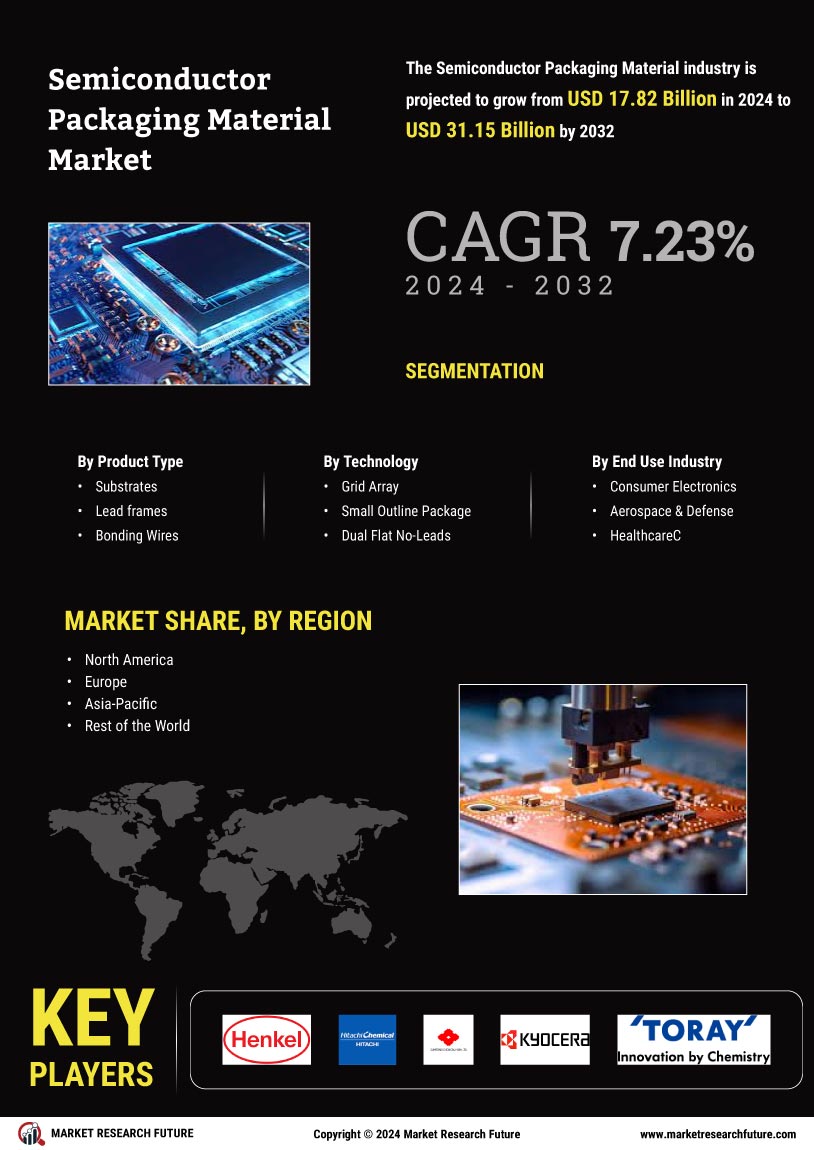
Certified Global Research Member
Isomar fd.webp Wcrc 57.webp
Key Questions Answered
  • Global Market Outlook
  • In-depth analysis of global and regional trends
  • Analyze and identify the major players in the market, their market share, key developments, etc.
  • To understand the capability of the major players based on products offered, financials, and strategies.
  • Identify disrupting products, companies, and trends.
  • To identify opportunities in the market.
  • Analyze the key challenges in the market.
  • Analyze the regional penetration of players, products, and services in the market.
  • Comparison of major players’ financial performance.
  • Evaluate strategies adopted by major players.
  • Recommendations
Why Choose Market Research Future?
  • Vigorous research methodologies for specific market.
  • Knowledge partners across the globe
  • Large network of partner consultants.
  • Ever-increasing/ Escalating data base with quarterly monitoring of various markets
  • Trusted by fortune 500 companies/startups/ universities/organizations
  • Large database of 5000+ markets reports.
  • Effective and prompt pre- and post-sales support.

Semiconductor Packaging Material Market Research Report Information By Product Type (Substrates, Lead Frames, Bonding Wires, Encapsulants, Underfill Materials, Die Attach, Solder Balls & Others), By Technology (Grid Array, Small Outline Package, Dual Flat No-Leads, Quad Flat Package, Dual In-Line Package & Others), By End-Use (Consumer Electronics, Aerospace & Defense, Healthcare, Communication, Automotive & Others) And By Region (North America, Europe, Asia-Pacific & Rest Of The World)– Industry Forecast Till 2032


ID: MRFR/SEM/0710-HCR | 115 Pages | Author: Ankit Gupta| April 2024

Semiconductor Packaging Material Product Type Outlook (USD Billion, 2018-2032)


  • Substrates


  • Lead frames


  • Bonding Wires


  • Encapsulants


  • Underfill Materials


  • Die Attach


  • Solder Balls


  • Wafer Level Packaging Dielectrics


  • Others


Semiconductor Packaging Material Technology Outlook (USD Billion, 2018-2032)


  • Grid Array


  • Small Outline Package


  • Dual Flat No-Leads


  • Quad Flat Package


  • Dual In-Line Package


  • Others


Semiconductor Packaging Material End Use Industry Outlook (USD Billion, 2018-2032)


  • Consumer Electronics


  • Aerospace & Defense


  • Healthcare


  • Communication


  • Automotive


  • Others


Semiconductor Packaging Material Regional Outlook (USD Billion, 2018-2032)


  • North America Outlook (USD Billion, 2018-2032)


    • North America Semiconductor Packaging Material by Product Type


      • Substrates


      • Lead frames


      • Bonding Wires


      • Encapsulants


      • Underfill Materials


      • Die Attach


      • Solder Balls


      • Wafer Level Packaging Dielectrics


      • Others


    • North America Semiconductor Packaging Material by Technology


      • Grid Array


      • Small Outline Package


      • Dual Flat No-Leads


      • Quad Flat Package


      • Dual In-Line Package


      • Others


    • North America Semiconductor Packaging Material by End Use Industry


      • Consumer Electronics


      • Aerospace & Defense


      • Healthcare


      • Communication


      • Automotive


      • Others


    • US Outlook (USD Billion, 2018-2032)


    • US Semiconductor Packaging Material by Product Type


      • Substrates


      • Lead frames


      • Bonding Wires


      • Encapsulants


      • Underfill Materials


      • Die Attach


      • Solder Balls


      • Wafer Level Packaging Dielectrics


      • Others


    • US Semiconductor Packaging Material by Technology


      • Grid Array


      • Small Outline Package


      • Dual Flat No-Leads


      • Quad Flat Package


      • Dual In-Line Package


      • Others


    • US Semiconductor Packaging Material by End Use Industry


      • Consumer Electronics


      • Aerospace & Defense


      • Healthcare


      • Communication


      • Automotive


      • Others


    • CANADA Outlook (USD Billion, 2018-2032)


    • CANADA Semiconductor Packaging Material by Product Type


      • Substrates


      • Lead frames


      • Bonding Wires


      • Encapsulants


      • Underfill Materials


      • Die Attach


      • Solder Balls


      • Wafer Level Packaging Dielectrics


      • Others


    • CANADA Semiconductor Packaging Material by Technology


      • Grid Array


      • Small Outline Package


      • Dual Flat No-Leads


      • Quad Flat Package


      • Dual In-Line Package


      • Others


    • CANADA Semiconductor Packaging Material by End Use Industry


      • Consumer Electronics


      • Aerospace & Defense


      • Healthcare


      • Communication


      • Automotive


      • Others


  • Europe Outlook (USD Billion, 2018-2032)


    • Europe Semiconductor Packaging Material by Product Type


      • Substrates


      • Lead frames


      • Bonding Wires


      • Encapsulants


      • Underfill Materials


      • Die Attach


      • Solder Balls


      • Wafer Level Packaging Dielectrics


      • Others


    • Europe Semiconductor Packaging Material by Technology


      • Grid Array


      • Small Outline Package


      • Dual Flat No-Leads


      • Quad Flat Package


      • Dual In-Line Package


      • Others


    • Europe Semiconductor Packaging Material by End Use Industry


      • Consumer Electronics


      • Aerospace & Defense


      • Healthcare


      • Communication


      • Automotive


      • Others


    • Germany Outlook (USD Billion, 2018-2032)


    • Germany Semiconductor Packaging Material by Product Type


      • Substrates


      • Lead frames


      • Bonding Wires


      • Encapsulants


      • Underfill Materials


      • Die Attach


      • Solder Balls


      • Wafer Level Packaging Dielectrics


      • Others


    • Germany Semiconductor Packaging Material by Technology


      • Grid Array


      • Small Outline Package


      • Dual Flat No-Leads


      • Quad Flat Package


      • Dual In-Line Package


      • Others


    • Germany Semiconductor Packaging Material by End Use Industry


      • Consumer Electronics


      • Aerospace & Defense


      • Healthcare


      • Communication


      • Automotive


      • Others


    • France Outlook (USD Billion, 2018-2032)


    • France Semiconductor Packaging Material by Product Type


      • Substrates


      • Lead frames


      • Bonding Wires


      • Encapsulants


      • Underfill Materials


      • Die Attach


      • Solder Balls


      • Wafer Level Packaging Dielectrics


      • Others


    • France Semiconductor Packaging Material by Technology


      • Grid Array


      • Small Outline Package


      • Dual Flat No-Leads


      • Quad Flat Package


      • Dual In-Line Package


      • Others


    • France Semiconductor Packaging Material by End Use Industry


      • Consumer Electronics


      • Aerospace & Defense


      • Healthcare


      • Communication


      • Automotive


      • Others


    • UK Outlook (USD Billion, 2018-2032)


    • UK Semiconductor Packaging Material by Product Type


      • Substrates


      • Lead frames


      • Bonding Wires


      • Encapsulants


      • Underfill Materials


      • Die Attach


      • Solder Balls


      • Wafer Level Packaging Dielectrics


      • Others


    • UK Semiconductor Packaging Material by Technology


      • Grid Array


      • Small Outline Package


      • Dual Flat No-Leads


      • Quad Flat Package


      • Dual In-Line Package


      • Others


    • UK Semiconductor Packaging Material by End Use Industry


      • Consumer Electronics


      • Aerospace & Defense


      • Healthcare


      • Communication


      • Automotive


      • Others


    • ITALY Outlook (USD Billion, 2018-2032)


    • ITALY Semiconductor Packaging Material by Product Type


      • Substrates


      • Lead frames


      • Bonding Wires


      • Encapsulants


      • Underfill Materials


      • Die Attach


      • Solder Balls


      • Wafer Level Packaging Dielectrics


      • Others


    • ITALY Semiconductor Packaging Material by Technology


      • Grid Array


      • Small Outline Package


      • Dual Flat No-Leads


      • Quad Flat Package


      • Dual In-Line Package


      • Others


    • ITALY Semiconductor Packaging Material by End Use Industry


      • Consumer Electronics


      • Aerospace & Defense


      • Healthcare


      • Communication


      • Automotive


      • Others


    • SPAIN Outlook (USD Billion, 2018-2032)


    • Spain Semiconductor Packaging Material by Product Type


      • Substrates


      • Lead frames


      • Bonding Wires


      • Encapsulants


      • Underfill Materials


      • Die Attach


      • Solder Balls


      • Wafer Level Packaging Dielectrics


      • Others


    • Spain Semiconductor Packaging Material by Technology


      • Grid Array


      • Small Outline Package


      • Dual Flat No-Leads


      • Quad Flat Package


      • Dual In-Line Package


      • Others


    • Spain Semiconductor Packaging Material by End Use Industry


      • Consumer Electronics


      • Aerospace & Defense


      • Healthcare


      • Communication


      • Automotive


      • Others


    • Rest Of Europe Outlook (USD Billion, 2018-2032)


    • Rest Of Europe Semiconductor Packaging Material by Product Type


      • Substrates


      • Lead frames


      • Bonding Wires


      • Encapsulants


      • Underfill Materials


      • Die Attach


      • Solder Balls


      • Wafer Level Packaging Dielectrics


      • Others


    • Rest Of Europe Semiconductor Packaging Material by Technology


      • Grid Array


      • Small Outline Package


      • Dual Flat No-Leads


      • Quad Flat Package


      • Dual In-Line Package


      • Others


    • Rest Of Europe Semiconductor Packaging Material by End Use Industry


      • Consumer Electronics


      • Aerospace & Defense


      • Healthcare


      • Communication


      • Automotive


      • Others


  • Asia-Pacific Outlook (USD Billion, 2018-2032)


    • Asia-Pacific Semiconductor Packaging Material by Product Type


      • Substrates


      • Lead frames


      • Bonding Wires


      • Encapsulants


      • Underfill Materials


      • Die Attach


      • Solder Balls


      • Wafer Level Packaging Dielectrics


      • Others


    • Asia-Pacific Semiconductor Packaging Material by Technology


      • Grid Array


      • Small Outline Package


      • Dual Flat No-Leads


      • Quad Flat Package


      • Dual In-Line Package


      • Others


    • Asia-Pacific Semiconductor Packaging Material by End Use Industry


      • Consumer Electronics


      • Aerospace & Defense


      • Healthcare


      • Communication


      • Automotive


      • Others


    • China Outlook (USD Billion, 2018-2032)


    • China Semiconductor Packaging Material by Product Type


      • Substrates


      • Lead frames


      • Bonding Wires


      • Encapsulants


      • Underfill Materials


      • Die Attach


      • Solder Balls


      • Wafer Level Packaging Dielectrics


      • Others


    • China Semiconductor Packaging Material by Technology


      • Grid Array


      • Small Outline Package


      • Dual Flat No-Leads


      • Quad Flat Package


      • Dual In-Line Package


      • Others


    • China Semiconductor Packaging Material by End Use Industry


      • Consumer Electronics


      • Aerospace & Defense


      • Healthcare


      • Communication


      • Automotive


      • Others


    • Japan Outlook (USD Billion, 2018-2032)


    • Japan Semiconductor Packaging Material by Product Type


      • Substrates


      • Lead frames


      • Bonding Wires


      • Encapsulants


      • Underfill Materials


      • Die Attach


      • Solder Balls


      • Wafer Level Packaging Dielectrics


      • Others


    • Japan Semiconductor Packaging Material by Technology


      • Grid Array


      • Small Outline Package


      • Dual Flat No-Leads


      • Quad Flat Package


      • Dual In-Line Package


      • Others


    • Japan Semiconductor Packaging Material by End Use Industry


      • Consumer Electronics


      • Aerospace & Defense


      • Healthcare


      • Communication


      • Automotive


      • Others


    • India Outlook (USD Billion, 2018-2032)


    • India Semiconductor Packaging Material by Product Type


      • Substrates


      • Lead frames


      • Bonding Wires


      • Encapsulants


      • Underfill Materials


      • Die Attach


      • Solder Balls


      • Wafer Level Packaging Dielectrics


      • Others


    • India Semiconductor Packaging Material by Technology


      • Grid Array


      • Small Outline Package


      • Dual Flat No-Leads


      • Quad Flat Package


      • Dual In-Line Package


      • Others


    • India Semiconductor Packaging Material by End Use Industry


      • Consumer Electronics


      • Aerospace & Defense


      • Healthcare


      • Communication


      • Automotive


      • Others


    • Australia Outlook (USD Billion, 2018-2032)


    • Australia Semiconductor Packaging Material by Product Type


      • Substrates


      • Lead frames


      • Bonding Wires


      • Encapsulants


      • Underfill Materials


      • Die Attach


      • Solder Balls


      • Wafer Level Packaging Dielectrics


      • Others


    • Australia Semiconductor Packaging Material by Technology


      • Grid Array


      • Small Outline Package


      • Dual Flat No-Leads


      • Quad Flat Package


      • Dual In-Line Package


      • Others


    • Australia Semiconductor Packaging Material by End Use Industry


      • Consumer Electronics


      • Aerospace & Defense


      • Healthcare


      • Communication


      • Automotive


      • Others


    • Rest of Asia-Pacific Outlook (USD Billion, 2018-2032)


    • Rest of Asia-Pacific Semiconductor Packaging Material by Product Type


      • Substrates


      • Lead frames


      • Bonding Wires


      • Encapsulants


      • Underfill Materials


      • Die Attach


      • Solder Balls


      • Wafer Level Packaging Dielectrics


      • Others


    • Rest of Asia-Pacific Semiconductor Packaging Material by Technology


      • Grid Array


      • Small Outline Package


      • Dual Flat No-Leads


      • Quad Flat Package


      • Dual In-Line Package


      • Others


    • Rest of Asia-Pacific Semiconductor Packaging Material by End Use Industry


      • Consumer Electronics


      • Aerospace & Defense


      • Healthcare


      • Communication


      • Automotive


      • Others


  • Rest of the World Outlook (USD Billion, 2018-2032)


    • Rest of the World Semiconductor Packaging Material by Product Type


      • Substrates


      • Lead frames


      • Bonding Wires


      • Encapsulants


      • Underfill Materials


      • Die Attach


      • Solder Balls


      • Wafer Level Packaging Dielectrics


      • Others


    • Rest of the World Semiconductor Packaging Material by Technology


      • Grid Array


      • Small Outline Package


      • Dual Flat No-Leads


      • Quad Flat Package


      • Dual In-Line Package


      • Others


    • Rest of the World Semiconductor Packaging Material by End Use Industry


      • Consumer Electronics


      • Aerospace & Defense


      • Healthcare


      • Communication


      • Automotive


      • Others


    • Middle East Outlook (USD Billion, 2018-2032)


    • Middle East Semiconductor Packaging Material by Product Type


      • Substrates


      • Lead frames


      • Bonding Wires


      • Encapsulants


      • Underfill Materials


      • Die Attach


      • Solder Balls


      • Wafer Level Packaging Dielectrics


      • Others


    • Middle East Semiconductor Packaging Material by Technology


      • Grid Array


      • Small Outline Package


      • Dual Flat No-Leads


      • Quad Flat Package


      • Dual In-Line Package


      • Others


    • Middle East Semiconductor Packaging Material by End Use Industry


      • Consumer Electronics


      • Aerospace & Defense


      • Healthcare


      • Communication


      • Automotive


      • Others


    • Africa Outlook (USD Billion, 2018-2032)


    • Africa Semiconductor Packaging Material by Product Type


      • Substrates


      • Lead frames


      • Bonding Wires


      • Encapsulants


      • Underfill Materials


      • Die Attach


      • Solder Balls


      • Wafer Level Packaging Dielectrics


      • Others


    • Africa Semiconductor Packaging Material by Technology


      • Grid Array


      • Small Outline Package


      • Dual Flat No-Leads


      • Quad Flat Package


      • Dual In-Line Package


      • Others


    • Africa Semiconductor Packaging Material by End Use Industry


      • Consumer Electronics


      • Aerospace & Defense


      • Healthcare


      • Communication


      • Automotive


      • Others


    • Latin America Outlook (USD Billion, 2018-2032)


    • Latin America Semiconductor Packaging Material by Product Type


      • Substrates


      • Lead frames


      • Bonding Wires


      • Encapsulants


      • Underfill Materials


      • Die Attach


      • Solder Balls


      • Wafer Level Packaging Dielectrics


      • Others


    • Latin America Semiconductor Packaging Material by Technology


      • Grid Array


      • Small Outline Package


      • Dual Flat No-Leads


      • Quad Flat Package


      • Dual In-Line Package


      • Others


    • Latin America Semiconductor Packaging Material by End Use Industry


      • Consumer Electronics


      • Aerospace & Defense


      • Healthcare


      • Communication


      • Automotive


      • Others


Leading companies partner with us for data-driven Insights
client_1 client_2 client_3 client_4 client_5 client_6 client_7 client_8 client_9 client_10
Please fill in Business Email for Quick Response

Table of Contents

1 Executive Summary

2 Scope of the Report

2.1 Market Definition

2.2 Scope of the Study

2.2.1 Definition

2.2.2 Research Objective

2.2.3 Assumptions

2.2.4 Limitations

2.3 Research Type

2.3.1 Primary Research

2.3.2 Secondary Research

2.4 Market size Estimation

2.5 Forecast Model

3 Market Landscape

3.1 Porter’s Five Forces Analysis

3.1.1 Threat of New Entrants

3.1.2 Bargaining power of buyers

3.1.3 Threat of substitutes

3.1.4 Segment rivalry

3.1.5 Bargaining Power of Buyers

3.2 Value Chain/Supply Chain Analysis

4 Market Dynamics

4.1 Introduction

4.2 Market Drivers

4.3 Market Restraints

4.4 Market Opportunities

4.5 Market Trends

5 Global Semiconductor Packaging Material Market, By Type

5.1 Introduction

5.2 Organic Substrates

5.2.1 Market Estimates & Forecast, 2023-2032

5.2.2 Market Estimates & Forecast by Region, 2023-2032

5.3 Bonding Wires

5.3.1 Market Estimates & Forecast, 2023-2032

5.3.2 Market Estimates & Forecast by Region, 2023-2032

5.4 Encapsulation Resins

5.4.1 Market Estimates & Forecast, 2023-2032

5.4.2 Market Estimates & Forecast by Region, 2023-2032

5.5 Ceramic Packages

5.5.1 Market Estimates & Forecast, 2023-2032

5.5.2 Market Estimates & Forecast by Region, 2023-2032

5.6 Solder Balls

5.6.1 Market Estimates & Forecast, 2023-2032

5.6.2 Market Estimates & Forecast by Region, 2023-2032

5.7 Wafer Level Packaging Dielectrics

5.7.1 Market Estimates & Forecast, 2023-2032

5.7.2 Market Estimates & Forecast by Region, 2023-2032

5.8 Others

5.8.1 Market Estimates & Forecast, 2023-2032

5.8.2 Market Estimates & Forecast by Region, 2023-2032

6 Global Semiconductor Packaging Material Market, By Technology

6.1 Introduction

6.2 Grid Array

6.2.1 Market Estimates & Forecast, 2023-2032

6.2.2 Market Estimates & Forecast by Region, 2023-2032

6.3 Small Outline Package

6.3.1 Market Estimates & Forecast, 2023-2032

6.3.2 Market Estimates & Forecast by Region, 2023-2032

6.4 Dual Flat No-Leads

6.4.1 Market Estimates & Forecast, 2023-2032

6.4.2 Market Estimates & Forecast by Region, 2023-2032

6.5 Quad Flat Package

6.5.1 Market Estimates & Forecast, 2023-2032

6.5.2 Market Estimates & Forecast by Region, 2023-2032

6.6 Dual In-Line Package

6.6.1 Market Estimates & Forecast, 2023-2032

6.6.2 Market Estimates & Forecast by Region, 2023-2032

6.7 Others

6.7.1 Market Estimates & Forecast, 2023-2032

6.7.2 Market Estimates & Forecast by Region, 2023-2032

7 Global Semiconductor Packaging Material Market, By Region

7.1 Introduction

7.2 North America

7.2.1 Market Estimates & Forecast, 2023-2032

7.2.2 Market Estimates & Forecast by Type, 2023-2032

7.2.3 Market Estimates & Forecast by Technology, 2023-2032

7.2.4 The U.S.

7.2.4.1 Market Estimates & Forecast, 2023-2032

7.2.4.2 Market Estimates & Forecast by Type, 2023-2032

7.2.4.3 Market Estimates & Forecast by Technology, 2023-2032

7.2.5 Canada

7.2.5.1 Market Estimates & Forecast, 2023-2032

7.2.5.2 Market Estimates & Forecast by Type, 2023-2032

7.2.5.3 Market Estimates & Forecast by Technology, 2023-2032

7.3 Europe

7.3.1 Market Estimates & Forecast, 2023-2032

7.3.2 Market Estimates & Forecast by Type, 2023-2032

7.3.3 Market Estimates & Forecast by Technology, 2023-2032

7.3.4 U.K.

7.3.4.1 Market Estimates & Forecast, 2023-2032

7.3.4.2 Market Estimates & Forecast by Type, 2023-2032

7.3.4.3 Market Estimates & Forecast by Technology, 2023-2032

7.3.5 Germany

7.3.5.1 Market Estimates & Forecast, 2023-2032

7.3.5.2 Market Estimates & Forecast by Type, 2023-2032

7.3.5.3 Market Estimates & Forecast by Technology, 2023-2032

7.3.6 France

7.3.6.1 Market Estimates & Forecast, 2023-2032

7.3.6.2 Market Estimates & Forecast by Type, 2023-2032

7.3.6.3 Market Estimates & Forecast by Technology, 2023-2032

7.3.7 Spain

7.3.7.1 Market Estimates & Forecast, 2023-2032

7.3.7.2 Market Estimates & Forecast by Type, 2023-2032

7.3.7.3 Market Estimates & Forecast by Technology, 2023-2032

7.3.8 Rest of Europe

7.3.8.1 Market Estimates & Forecast, 2023-2032

7.3.8.2 Market Estimates & Forecast by Type, 2023-2032

7.3.8.3 Market Estimates & Forecast by Technology, 2023-2032

7.4 Asia Pacific

7.4.1 Market Estimates & Forecast, 2023-2032

7.4.2 Market Estimates & Forecast by Type, 2023-2032

7.4.3 Market Estimates & Forecast by Technology, 2023-2032

7.4.4 China

7.4.4.1 Market Estimates & Forecast, 2023-2032

7.4.4.2 Market Estimates & Forecast by Type, 2023-2032

7.4.4.3 Market Estimates & Forecast by Technology, 2023-2032

7.4.5 India

7.4.5.1 Market Estimates & Forecast, 2023-2032

7.4.5.2 Market Estimates & Forecast by Type, 2023-2032

7.4.5.3 Market Estimates & Forecast by Technology, 2023-2032

7.4.6 Japan

7.4.6.1 Market Estimates & Forecast, 2023-2032

7.4.6.2 Market Estimates & Forecast by Type, 2023-2032

7.4.6.3 Market Estimates & Forecast by Technology, 2023-2032

7.4.7 South Korea

7.4.7.1 Market Estimates & Forecast, 2023-2032

7.4.7.2 Market Estimates & Forecast by Type, 2023-2032

7.4.7.3 Market Estimates & Forecast by Technology, 2023-2032

7.4.8 Australia

7.4.8.1 Market Estimates & Forecast, 2023-2032

7.4.8.2 Market Estimates & Forecast by Type, 2023-2032

7.4.8.3 Market Estimates & Forecast by Technology, 2023-2032

7.4.9 Rest of Asia Pacific

7.4.9.1 Market Estimates & Forecast, 2023-2032

7.4.9.2 Market Estimates & Forecast by Type, 2023-2032

7.4.9.3 Market Estimates & Forecast by Technology, 2023-2032

7.5 Middle East & Africa

7.5.1 Market Estimates & Forecast, 2023-2032

7.5.2 Market Estimates & Forecast by Type, 2023-2032

7.5.3 Market Estimates & Forecast by Technology, 2023-2032

8 Competitive Landscape

9 Company Profile

9.1 Henkel AG & Company, KGaA

9.1.1 Company Overview

9.1.2 Types/Services Offering

9.1.3 Financial Overview

9.1.4 Key Developments

9.1.5 Strategy

9.1.6 SWOT Analysis

9.2 Hitachi Chemical Company, Ltd.

9.2.1 Company Overview

9.2.2 Types/Services Offering

9.2.3 Financial Overview

9.2.4 Key Developments

9.2.5 Strategy

9.2.6 SWOT Analysis

9.3 Sumitomo Chemical Co., Ltd.

9.3.1 Company Overview

9.3.2 Types/Services Offering

9.3.3 Financial Overview

9.3.4 Key Developments

9.3.5 Strategy

9.3.6 SWOT Analysis

9.4 Kyocera Chemical Corporation

9.4.1 Company Overview

9.4.2 Types/Services Offering

9.4.3 Financial Overview

9.4.4 Key Developments

9.4.5 Strategy

9.4.6 SWOT Analysis

9.5 Mitsui High-tec, Inc.

9.5.1 Company Overview

9.5.2 Types/Services Offering

9.5.3 Financial Overview

9.5.4 Key Developments

9.5.5 Strategy

9.5.6 SWOT Analysis

9.6 Toray Industries, Inc.

9.6.1 Company Overview

9.6.2 Types/Services Offering

9.6.3 Financial Overview

9.6.4 Key Developments

9.6.5 Strategy

9.6.6 SWOT Analysis

9.7 Alent plc

9.7.1 Company Overview

9.7.2 Types/Services Offering

9.7.3 Financial Overview

9.7.4 Key Developments

9.7.5 Strategy

9.7.6 SWOT Analysis

9.8 LG Chem

9.8.1 Company Overview

9.8.2 Types/Services Offering

9.8.3 Financial Overview

9.8.4 Key Developments

9.8.5 Strategy

9.8.6 SWOT Analysis

9.9 BASF SE

9.9.1 Company Overview

9.9.2 Types/Services Offering

9.9.3 Financial Overview

9.9.4 Key Developments

9.9.5 Strategy

9.9.6 SWOT Analysis

9.10 Tanaka Kikinzoku Group

9.10.1 Company Overview

9.10.2 Types/Services Offering

9.10.3 Financial Overview

9.10.4 Key Developments

9.10.5 Strategy

9.10.6 SWOT Analysis

9.11 E. I. du Pont de Nemours and Company

9.11.1 Company Overview

9.11.2 Types/Services Offering

9.11.3 Financial Overview

9.11.4 Key Developments

9.11.5 Strategy

9.11.6 SWOT Analysis

9.12 Honeywell International Inc.

9.12.1 Company Overview

9.12.2 Types/Services Offering

9.12.3 Financial Overview

9.12.4 Key Developments

9.12.5 Strategy

9.12.6 SWOT Analysis

9.13 Toppan Printing Co., Ltd.

9.13.1 Company Overview

9.13.2 Types/Services Offering

9.13.3 Financial Overview

9.13.4 Key Developments

9.13.5 Strategy

9.13.6 SWOT Analysis

9.14 Nippon Micrometal Corporation

9.14.1 Company Overview

9.14.2 Types/Services Offering

9.14.3 Financial Overview

9.14.4 Key Developments

9.14.5 Strategy

9.14.6 SWOT Analysis

9.15 Alpha Advanced Materials

9.15.1 Company Overview

9.15.2 Types/Services Offering

9.15.3 Financial Overview

9.15.4 Key Developments

9.15.5 Strategy

9.15.6 SWOT Analysis

List of Tables

Table 1 Global Semiconductor Packaging Material Market: By Region, 2023-2032

Table 2 North America Semiconductor Packaging Material Market: By Country, 2023-2032

Table 3 Europe Semiconductor Packaging Material Market: By Country, 2023-2032

Table 4 Asia-Pacific Semiconductor Packaging Material Market: By Country, 2023-2032

Table 5 RoW Semiconductor Packaging Material Market: By Country, 2023-2032

Table 6 Global Semiconductor Packaging Material Market, By Type, By Regions, 2023-2032

Table 7 North America Semiconductor Packaging Material Market, By Type, By Country, 2023-2032

Table 8 Europe Semiconductor Packaging Material Market, By Type, By Country, 2023-2032

Table 9 Asia-Pacific Semiconductor Packaging Material Market By Type, By Country, 2023-2032

Table 10 RoW Semiconductor Packaging Material Market By Type, By Country, 2023-2032

Table 11 Global Ambient Food Packaging By Technology Market: By Regions, 2023-2032

Table 12 North America Semiconductor Packaging Material Market By Technology : By Country, 2023-2032

Table 13 Europe Semiconductor Packaging Material Market By Technology : By Country, 2023-2032

Table 14 Asia Pacific Semiconductor Packaging Material Market By Technology : By Country, 2023-2032

Table 15 RoW Semiconductor Packaging Material Market By Technology : By Country, 2023-2032

Table 16 Global Semiconductor Packaging Material Market: By Region, 2023-2032

Table 17 Global Semiconductor Packaging Material Market: By Type, 2023-2032

Table 18 Global Semiconductor Packaging Material Market: By Technology, 2023-2032

Table 19 North America Semiconductor Packaging Material Market, By Country

Table 20 North America Semiconductor Packaging Material Market, By Type

Table 21 North America Semiconductor Packaging Material Market, By Technology

Table 22 Europe: Semiconductor Packaging Material Market, By Country

Table 23 Europe: Semiconductor Packaging Material Market, By Type

Table 24 Europe: Semiconductor Packaging Material Market, By Technology

Table 25 Asia-Pacific: Semiconductor Packaging Material Market, By Country

Table 26 Asia-Pacific: Semiconductor Packaging Material Market, By Type

Table 27 Asia-Pacific: Semiconductor Packaging Material Market, By End-User

Table 28 RoW: Semiconductor Packaging Material Market, By Region

Table 29 RoW Semiconductor Packaging Material Market, By Type

Table 30 RoW Semiconductor Packaging Material Market, By Technology

List of Figures

FIGURE 1 RESEARCH TYPEOF MRFR

FIGURE 2 TOP DOWN & BOTTOM UP APPROACH

FIGURE 3 Market Dynamics

FIGURE 4 impact analysis: market drivers

FIGURE 5 impact analysis: market restraints

FIGURE 6 porter’s five forces analysis

FIGURE 7 Value chain analysis

FIGURE 8 Global Semiconductor Packaging Material Market SHARE, By Type, 2020 (%)

FIGURE 9 Global Semiconductor Packaging Material Market, By Type, 2023-2032 (USD MILLION)

FIGURE 10 Global Semiconductor Packaging Material Market SHARE, By Technology, 2020 (%)

FIGURE 11 Global Semiconductor Packaging Material Market, By Technology, 2023-2032 (USD MILLION)

FIGURE 12 Global Semiconductor Packaging Material Market SHARE (%), BY REGION, 2020

FIGURE 13 Global Semiconductor Packaging Material Market, BY REGION, 2023-2032 (USD MILLION)

FIGURE 14 North America Semiconductor Packaging Material SHARE (%), 2020

FIGURE 15 North America Semiconductor Packaging Material Market BY Country, 2023-2032 (USD MILLION)

FIGURE 16 Europe Semiconductor Packaging Material Market SHARE (%), 2020

FIGURE 17 Europe Semiconductor Packaging Material Market BY Country, 2023-2032 (USD MILLION)

FIGURE 18 Asia-Pacific Semiconductor Packaging Material Market SHARE (%), 2020

FIGURE 19 Asia-Pacific Semiconductor Packaging Material Market BY Country, 2023-2032 (USD MILLION)

FIGURE 20 Rest of the World Semiconductor Packaging Material Market SHARE (%), 2020

FIGURE 21 Rest of the World Semiconductor Packaging Material Market BY Country, 2023-2032 (USD MILLION)

Purchase Option
Single User $ 4,950
Multiuser License $ 5,950
Enterprise User $ 7,250
Compare Licenses
Tailored for You
  • Dedicated Research on any specifics segment or region.
  • Focused Research on specific players in the market.
  • Custom Report based only on your requirements.
  • Flexibility to add or subtract any chapter in the study.
  • Historic data from 2014 and forecasts outlook till 2040.
  • Flexibility of providing data/insights in formats (PDF, PPT, Excel).
  • Provide cross segmentation in applicable scenario/markets.