×
Request Free Sample ×

Kindly complete the form below to receive a free sample of this Report

* Please use a valid business email

Leading companies partner with us for data-driven Insights

clients tt-cursor
Hero Background

3D IC 2.5D IC Packaging Market

ID: MRFR/SEM/30156-HCR
128 Pages
Aarti Dhapte
October 2025

3D IC and 2.5D IC Packaging Market Research Report By Packaging Technology (Wafer Level Package, Fan-Out Package, Through-Silicon Via (TSV), System in Package (SiP)), By Material Type (Silicon, Ceramics, Polymer, Metal), By Application (Consumer Electronics, Telecommunications, Automotive, Industrial), By Form Factor (2D Packaging, 3D Packaging, 2.5D Packaging), By Integration Type (Heterogeneous Integration, Homogeneous Integration) and By Region (North America, Europe, South America, Asia Pacific, Middle East and Africa) - Forecast to 2035

Share:
Download PDF ×

We do not share your information with anyone. However, we may send you emails based on your report interest from time to time. You may contact us at any time to opt-out.

3D IC 2.5D IC Packaging Market Infographic
Purchase Options

3D IC 2.5D IC Packaging Market Summary

As per MRFR analysis, the 3D IC and 2.5D IC Packaging Market was estimated at 24.61 USD Billion in 2024. The 3D IC and 2.5D IC Packaging industry is projected to grow from 25.96 USD Billion in 2025 to 44.13 USD Billion by 2035, exhibiting a compound annual growth rate (CAGR) of 5.45 during the forecast period 2025 - 2035.

Key Market Trends & Highlights

The 3D IC and 2.5D IC Packaging Market is poised for substantial growth driven by technological advancements and increasing application demands.

  • The integration of advanced materials is becoming a pivotal trend in enhancing packaging performance.
  • Sustainability initiatives are gaining traction, influencing design and manufacturing processes across the industry.
  • Heterogeneous integration is emerging as a key focus, enabling diverse functionalities within compact form factors.
  • Rising demand for high-performance computing and advancements in semiconductor technology are major drivers propelling market expansion.

Market Size & Forecast

2024 Market Size 24.61 (USD Billion)
2035 Market Size 44.13 (USD Billion)
CAGR (2025 - 2035) 5.45%

Major Players

TSMC (TW), Intel (US), Samsung (KR), Micron Technology (US), GlobalFoundries (US), ASE Technology Holding Co. (TW), STMicroelectronics (FR), NXP Semiconductors (NL), Texas Instruments (US)

3D IC 2.5D IC Packaging Market Trends

The 3D IC and 2.5D IC Packaging Market is currently experiencing a transformative phase, driven by the increasing demand for advanced semiconductor technologies. This market is characterized by the integration of multiple chips into a single package, which enhances performance and reduces power consumption. As industries such as consumer electronics, automotive, and telecommunications continue to evolve, the need for compact and efficient packaging solutions becomes more pronounced. The trend towards miniaturization and the Internet of Things (IoT) further propels the adoption of these innovative packaging techniques, suggesting a robust growth trajectory for the market. Moreover, the ongoing advancements in manufacturing processes and materials are likely to play a pivotal role in shaping the future landscape of the 3D IC and 2.5D IC Packaging Market. Companies are increasingly investing in research and development to enhance the reliability and scalability of these technologies. This focus on innovation, coupled with the rising complexity of electronic systems, indicates that the market will continue to expand, catering to the diverse needs of various sectors. As the global economy becomes more interconnected, the implications of these developments are expected to resonate across multiple industries, highlighting the strategic importance of this market in the broader technological ecosystem.

Integration of Advanced Materials

The 3D IC and 2.5D IC Packaging Market is witnessing a shift towards the use of advanced materials that enhance thermal performance and electrical efficiency. This trend indicates a growing emphasis on materials that can withstand higher temperatures and provide better conductivity, which is essential for high-performance applications.

Focus on Sustainability

Sustainability is becoming a central theme in the 3D IC and 2.5D IC Packaging Market, as manufacturers seek to reduce waste and energy consumption. This focus suggests a potential shift towards eco-friendly materials and processes, aligning with global environmental goals and consumer preferences.

Emergence of Heterogeneous Integration

Heterogeneous integration is gaining traction within the 3D IC and 2.5D IC Packaging Market, as it allows for the combination of different technologies and functionalities within a single package. This trend may lead to more versatile and powerful electronic devices, catering to the diverse demands of modern applications.

3D IC 2.5D IC Packaging Market Drivers

Expansion of Automotive Electronics

The expansion of automotive electronics is emerging as a crucial driver for the 3D IC and 2.5D IC Packaging Market. With the rise of electric vehicles and advanced driver-assistance systems, the demand for sophisticated semiconductor solutions is on the rise. 3D IC and 2.5D IC packaging technologies enable the integration of multiple functionalities within compact spaces, which is essential for modern automotive applications. The automotive semiconductor market is projected to grow significantly, with estimates indicating it could reach USD 50 billion by 2027. This growth is likely to spur the adoption of 3D IC and 2.5D IC packaging solutions, as manufacturers seek to enhance performance and reliability in automotive electronics.

Increased Focus on Energy Efficiency

The growing emphasis on energy efficiency in electronic devices is driving the 3D IC and 2.5D IC Packaging Market. As consumers and industries alike become more environmentally conscious, there is a rising demand for semiconductor solutions that minimize power consumption while maximizing performance. 3D IC and 2.5D IC packaging technologies are designed to reduce energy usage through improved thermal management and reduced interconnect lengths. This focus on energy efficiency is reflected in market trends, with energy-efficient semiconductor solutions expected to capture a larger share of the market. As regulations and consumer preferences shift towards sustainability, the adoption of these advanced packaging technologies is likely to increase.

Advancements in Semiconductor Technology

Technological advancements in semiconductor manufacturing processes are significantly influencing the 3D IC and 2.5D IC Packaging Market. Innovations such as extreme ultraviolet lithography and advanced packaging techniques are enabling the production of smaller, more powerful chips. These advancements facilitate the integration of multiple functionalities within a single package, thereby enhancing performance and reducing power consumption. The market for semiconductor packaging is expected to reach approximately USD 40 billion by 2026, driven by these technological improvements. As manufacturers strive to meet the increasing demands for miniaturization and efficiency, the adoption of 3D IC and 2.5D IC packaging solutions is likely to accelerate.

Rising Demand for High-Performance Computing

The increasing demand for high-performance computing solutions is a primary driver for the 3D IC and 2.5D IC Packaging Market. As industries such as artificial intelligence, machine learning, and data analytics expand, the need for advanced semiconductor technologies becomes more pronounced. The 3D IC and 2.5D IC packaging solutions offer enhanced performance and efficiency, which are critical for processing large volumes of data. According to recent estimates, the market for high-performance computing is projected to grow at a compound annual growth rate of over 10% in the coming years. This growth is likely to propel the adoption of 3D IC and 2.5D IC packaging technologies, as they provide the necessary speed and power efficiency required for modern computing applications.

Growing Internet of Things (IoT) Applications

The proliferation of Internet of Things (IoT) devices is a significant driver for the 3D IC and 2.5D IC Packaging Market. As more devices become interconnected, the demand for efficient and compact semiconductor solutions rises. 3D IC and 2.5D IC packaging technologies provide the necessary integration and performance enhancements required for IoT applications, which often involve processing large amounts of data in real-time. The IoT market is anticipated to grow substantially, with estimates suggesting it could reach USD 1 trillion by 2025. This growth is likely to create substantial opportunities for 3D IC and 2.5D IC packaging solutions, as manufacturers seek to optimize their products for performance and energy efficiency.

Market Segment Insights

By Packaging Technology: Wafer Level Package (Largest) vs. Fan-Out Package (Fastest-Growing)

In the 3D IC and 2.5D IC Packaging Market, Wafer Level Package (WLP) holds the largest market share due to its ability to provide high-density interconnections and compact designs. This technology enables multiple dies to be integrated into a single package, enhancing performance and reducing size. Fan-Out Package, while currently smaller in market share, is recognized as the fastest-growing segment, driven by increasing demand for high-performance computing and mobile devices that require advanced packaging solutions. The growth of the Fan-Out Package segment is largely attributed to technological advancements that allow for larger die sizes and better thermal performance. This trend is fueled by the increasing need for efficient packaging solutions that can support the rising complexity of integrated circuits. Moreover, the demand for smaller and more efficient devices is pushing manufacturers to focus on innovative packaging technologies, making Fan-Out a promising area for future investment and development.

Wafer Level Package (Dominant) vs. Through-Silicon Via (TSV) (Emerging)

Wafer Level Packaging (WLP) is recognized for its dominance in the 3D IC and 2.5D IC Packaging Market due to its cost-effectiveness and efficiency in the fabrication process. This technology facilitates high integration density and improved electrical performance by reducing the distance between the chip and package. In contrast, Through-Silicon Via (TSV) is an emerging technology that supports vertical stacking of dies, thus allowing for the greater interconnectivity essential for advanced applications. Although TSV currently holds a smaller market position, its ability to enhance signal integrity and reduce latency makes it a compelling option for future applications that demand high-speed data transfer and efficient thermal management.

By Material Type: Silicon (Largest) vs. Ceramics (Fastest-Growing)

The 3D IC and 2.5D IC packaging market showcases a diverse material type distribution, with silicon leading as the most significant segment. Silicon's substantial presence is attributed to its robust electrical properties and compatibility with existing semiconductor manufacturing processes. Ceramics are emerging rapidly, showing a notable share due to their thermal stability and low dielectric constant, making them highly suitable for advanced packaging solutions. Growth trends in the material type segment reflect a dynamic market influenced by technological advancements and increasing demand for miniaturization in electronics. Silicon continues to dominate due to its established use in IC fabrication, while ceramics are gaining traction as industries seek to enhance performance and reliability. The polymer and metal segments also contribute to this evolving landscape, each offering distinct advantages for specific applications.

Silicon (Dominant) vs. Metallurgy (Emerging)

Silicon, as the dominant material in the 3D IC and 2.5D IC packaging market, is characterized by its extensive use in traditional semiconductor devices. Its electrical properties make it an ideal choice for performance-driven applications. Meanwhile, the metallurgy segment is emerging, primarily focused on innovative packaging which includes metal substrates that enhance thermal conductivity. This is particularly appealing in high-power applications where heat dissipation is critical. As manufacturers strive for higher performance and lower power consumption, the flexibility and efficiency provided by metallurgical materials position them favorably in evolving applications, especially in next-gen electronics.

By Application: Consumer Electronics (Largest) vs. Automotive (Fastest-Growing)

The 3D IC and 2.5D IC Packaging Market exhibit a diverse application segment, with Consumer Electronics commanding the largest share. This category includes smartphones, tablets, and wearable devices, where the demand for miniaturization and performance enhancement drives the adoption of advanced packaging technologies. Telecommunications follows closely, leveraging the need for high-speed data transfer and efficient communication solutions. Meanwhile, the Automotive and Industrial applications are also significant players, contributing to a balanced market where various sectors influence the growth dynamics.

Consumer Electronics (Dominant) vs. Automotive (Emerging)

The Consumer Electronics segment is the dominant force in the 3D IC and 2.5D IC packaging market, characterized by rapid technological advancements and a strong focus on consumer demands for compact, high-performance devices. This segment heavily relies on innovations that enhance power efficiency and processing capabilities while reducing form factors. Conversely, the Automotive domain is emerging rapidly, propelled by trends towards electric vehicles and advanced driver-assistance systems (ADAS). As automotive manufacturers seek to integrate more functionalities into smaller spaces, the demand for sophisticated packaging solutions is poised to soar, making it a critical area of growth in the coming years.

By Form Factor: 2D Packaging (Largest) vs. 3D Packaging (Fastest-Growing)

In the 3D IC and 2.5D IC Packaging Market, the 2D Packaging segment holds the largest share, showcasing its established position and widespread application in various industries. This dominance is primarily attributed to its cost-effectiveness, simplicity in design, and compatibility with existing manufacturing practices. On the other hand, 3D packaging is rapidly gaining traction due to its ability to integrate multiple functionalities within a smaller footprint, making it increasingly preferred for advanced semiconductor applications. The growth of the 3D packaging segment is driven by the escalating demand for miniaturized electronic devices and higher performance requirements across sectors such as telecommunications, computing, and consumer electronics. This trend is further fueled by innovations in manufacturing technologies and material science, enhancing the feasibility and affordability of 3D integration solutions. Consequently, 3D packaging is expected to see the fastest growth as it becomes essential for meeting the evolving needs of modern electronic applications.

2D Packaging (Dominant) vs. 2.5D Packaging (Emerging)

The 2D Packaging segment remains dominant in the 3D IC and 2.5D IC Packaging Market, known for its simplicity and widespread applicability. 2D packaging has been the cornerstone of semiconductor manufacture, offering reliability and cost savings, which resonates well with manufacturers. In contrast, 2.5D Packaging represents an emerging technology that allows for enhanced connectivity and integration of multiple chips on a single substrate, thus bridging the gap between traditional 2D and cutting-edge 3D technologies. While 2D packaging faces limitations in terms of scaling performance, 2.5D packaging offers a strategic advantage in delivering improved power efficiency and performance at reduced latency. As the market shifts towards more integrated solutions, 2.5D packaging is positioning itself as a vital enabler for next-generation electronic devices.

By Integration Type: Heterogeneous Integration (Largest) vs. Homogeneous Integration (Fastest-Growing)

The 3D IC and 2.5D IC Packaging Market reveals that Heterogeneous Integration currently holds the largest market share among integration types. This method stands out due to its ability to combine different materials and components in a single package, catering to a wide range of applications in sectors like telecommunications and computing. In contrast, Homogeneous Integration, while not as widely adopted, is showing promise and is expected to capture an increasing share as technology advancements allow for more efficient manufacturing processes.

Integration Type: Heterogeneous Integration (Dominant) vs. Homogeneous Integration (Emerging)

Heterogeneous Integration is characterized by its capability to integrate disparate components, such as logic, memory, and sensors, into one compact package, which is essential for high-performance computing. This integration type addresses the demand for miniaturization and enhanced functionality in electronic devices. On the other hand, Homogeneous Integration focuses on the same types of materials, ensuring compatibility and efficiency in production. Although it currently lags behind Heterogeneous Integration, the increasing need for high-density packaging drives its growth, which is further supported by advancements in semiconductor technology and manufacturing processes.

Get more detailed insights about 3D IC 2.5D IC Packaging Market

Regional Insights

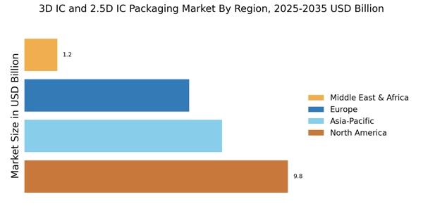
The 3D IC and 2.5D IC Packaging Market has shown a noteworthy distribution across various regions, with North America leading in valuation, reaching 9.32 USD Billion in 2023 and expected to grow to 14.51 USD Billion by 2032. This region's dominance is fueled by its advanced technology ecosystem and high demand for innovative packaging solutions. Europe, valued at 5.19 USD Billion in 2023, reflects significant market growth driven by increasing investments in semiconductor technologies, with projections of reaching 8.11 USD Billion by 2032.

The Asia Pacific region also plays a crucial role, valued at 6.09 USD Billion in 2023, and it is anticipated to grow to 10.03 USD Billion by 2032, supported by robust manufacturing bases and technological advancements. South America and the Middle East Africa are comparatively smaller markets, with valuations of 0.86 USD Billion and 0.67 USD Billion in 2023, respectively. However, both regions are experiencing growth opportunities due to increasing technology adoption.

Overall, the market exhibits a diverse segmentation, where North America and the Asia Pacific showcase the majority holding, while the emerging markets of South America and MEA signify potential for future expansion within the 3D IC and 2.5D IC Packaging Market industry.

3D IC 2.5D IC Packaging Market Regional Image

Key Players and Competitive Insights

The 3D IC and 2.5D IC Packaging Market is characterized by rapid advancements in technology and increasing demand for high-performance computing devices. As industries adopt more complex semiconductor technologies, the need for innovative packaging solutions becomes critical. These packaging types enhance the performance and integration of multiple chips within a single package, enabling improvements in speed, power efficiency, and size reduction. Competitive insights reveal that companies are focused on research and development to create cutting-edge packaging techniques, which is essential in staying ahead in a market that is continuously evolving with new players entering and existing ones expanding their capabilities. 

The driving factors behind the competitive landscape also include strategic partnerships, collaborations, and mergers aimed at enhancing product offerings and market reach.ASE Group stands as a prominent player in the 3D IC and 2.5D IC Packaging Market, leveraging its extensive experience and technological expertise. Known for its leadership in advanced packaging solutions, ASE Group has established a significant market presence fueled by strong customer relationships and a commitment to quality. Its strengths lie in its robust manufacturing capabilities, which allow for high-volume production of sophisticated packaging types.

The company continuously invests in state-of-the-art facilities and innovative processes that position it favorably against competitors. 

Moreover, ASE Group's proactive approach to exploring new materials and techniques enhances its product portfolio, enabling it to meet the demands of next-generation electronic devices in a way that resonates with industry trends for miniaturization and performance enhancement.TSMC is another key contributor to the 3D IC and 2.5D IC Packaging Market and is known for its cutting-edge technological advancements. The company's pioneering efforts in semiconductor manufacturing and packaging have set high industry standards, particularly in adopting 3D and 2.5D integration techniques. 

TSMC's strengths are reflected in its substantial investment in research and development, which has allowed it to innovate continuously and offer advanced packaging solutions that improve device performance and reliability. By fostering collaborations with various technology firms and enhancing its supply chain efficiencies, TSMC has solidified its position within the competitive landscape of the market. Additionally, TSMC's commitment to sustainability and eco-friendly practices resonates well with modern consumer expectations, further enhancing its brand reputation and market share within the 3D IC and 2.5D IC Packaging sectors.

Key Companies in the 3D IC 2.5D IC Packaging Market market include

Industry Developments

The 3D IC and 2.5D IC Packaging Market has recently witnessed significant advancements driven by technological innovation and increasing demand for high-performance electronics. Key players are investing heavily in research and development to enhance packaging efficiency and integration density, catering to industries such as consumer electronics, automotive, and telecommunications.

The ongoing transition toward miniaturized and energy-efficient devices has further accelerated the adoption of advanced packaging solutions. Recent collaborations among semiconductor manufacturers and notable entries into the market have aimed to address the challenges of thermal management and signal integrity in these packaging technologies.

Additionally, geopolitical factors and supply chain disruptions continue to influence manufacturing strategies and market dynamics, prompting companies to diversify their operations. As companies look to establish a competitive edge, sustainability initiatives are also gaining traction, focusing on reducing the environmental impact of manufacturing processes. This evolving landscape showcases the importance of adaptability and innovation in meeting the growing demands of the technology sector over the next few years.

Future Outlook

3D IC 2.5D IC Packaging Market Future Outlook

The 3D IC and 2.5D IC Packaging Market is projected to grow at a 5.45% CAGR from 2024 to 2035, driven by advancements in semiconductor technology and increasing demand for high-performance computing.

New opportunities lie in:

  • Development of advanced thermal management solutions for 3D ICs.
  • Integration of AI-driven design tools for efficient packaging processes.
  • Expansion into emerging markets with tailored packaging solutions.

By 2035, the market is expected to solidify its position as a leader in semiconductor packaging.

Market Segmentation

3D IC 2.5D IC Packaging Market Application Outlook

  • Consumer Electronics
  • Telecommunications
  • Automotive
  • Industrial

3D IC 2.5D IC Packaging Market Form Factor Outlook

  • 2D Packaging
  • 3D Packaging
  • 2.5D Packaging

3D IC 2.5D IC Packaging Market Material Type Outlook

  • Silicon
  • Ceramics
  • Polymer
  • Metal

3D IC 2.5D IC Packaging Market Integration Type Outlook

  • Heterogeneous Integration
  • Homogeneous Integration

3D IC 2.5D IC Packaging Market Packaging Technology Outlook

  • Wafer Level Package
  • Fan-Out Package
  • Through-Silicon Via (TSV)
  • System in Package (SiP)

Report Scope

MARKET SIZE 202424.61(USD Billion)
MARKET SIZE 202525.96(USD Billion)
MARKET SIZE 203544.13(USD Billion)
COMPOUND ANNUAL GROWTH RATE (CAGR)5.45% (2024 - 2035)
REPORT COVERAGERevenue Forecast, Competitive Landscape, Growth Factors, and Trends
BASE YEAR2024
Market Forecast Period2025 - 2035
Historical Data2019 - 2024
Market Forecast UnitsUSD Billion
Key Companies ProfiledMarket analysis in progress
Segments CoveredMarket segmentation analysis in progress
Key Market OpportunitiesAdvancements in miniaturization and integration drive demand in the 3D IC and 2.5D IC Packaging Market.
Key Market DynamicsTechnological advancements drive competitive forces in 3D IC and 2.5D IC packaging, enhancing performance and efficiency.
Countries CoveredNorth America, Europe, APAC, South America, MEA

Leave a Comment

FAQs

What is the projected market valuation for the 3D IC and 2.5D IC Packaging Market in 2035?

The projected market valuation for the 3D IC and 2.5D IC Packaging Market in 2035 is 44.13 USD Billion.

What was the market valuation for the 3D IC and 2.5D IC Packaging Market in 2024?

The market valuation for the 3D IC and 2.5D IC Packaging Market in 2024 was 24.61 USD Billion.

What is the expected CAGR for the 3D IC and 2.5D IC Packaging Market during the forecast period 2025 - 2035?

The expected CAGR for the 3D IC and 2.5D IC Packaging Market during the forecast period 2025 - 2035 is 5.45%.

Which companies are considered key players in the 3D IC and 2.5D IC Packaging Market?

Key players in the market include TSMC, Intel, Samsung, Micron Technology, GlobalFoundries, ASE Technology Holding Co., STMicroelectronics, NXP Semiconductors, and Texas Instruments.

What are the projected values for the Fan-Out Package segment by 2035?

The projected value for the Fan-Out Package segment is expected to reach 12.0 USD Billion by 2035.

How does the 3D Packaging segment compare to the 2D Packaging segment in terms of projected valuation for 2035?

The 3D Packaging segment is projected to reach 18.0 USD Billion, whereas the 2D Packaging segment is expected to reach 14.0 USD Billion by 2035.

What is the anticipated growth for the Through-Silicon Via (TSV) segment by 2035?

The Through-Silicon Via (TSV) segment is anticipated to grow to 14.0 USD Billion by 2035.

What is the projected valuation for the Consumer Electronics application segment in 2035?

The projected valuation for the Consumer Electronics application segment is expected to be 15.0 USD Billion by 2035.

What are the expected values for the Heterogeneous Integration segment by 2035?

The Heterogeneous Integration segment is expected to reach 22.07 USD Billion by 2035.

What is the projected value for the Silicon material type segment in 2035?

The projected value for the Silicon material type segment is expected to be 18.0 USD Billion by 2035.

Download Free Sample

Kindly complete the form below to receive a free sample of this Report

Compare Licence

×
Features License Type
Single User Multiuser License Enterprise User
Price $4,950 $5,950 $7,250
Maximum User Access Limit 1 User Upto 10 Users Unrestricted Access Throughout the Organization
Free Customization
Direct Access to Analyst
Deliverable Format
Platform Access
Discount on Next Purchase 10% 15% 15%
Printable Versions