Embedded Die Packaging Technologie Markt

Marktforschungsbericht zur Technologie der eingebetteten Die-Verpackung nach Anwendung (Konsumgüter, Telekommunikation, Automobil, Industrie), nach Verpackungsart (Fan-Out-Wafer-Level-Verpackung, Eingebettete-Wafer-Level-Verpackung, 2,5D-Verpackung, 3D-Verpackung), nach Materialart (Silizium, organische Substrate, Keramik, Polymer), nach Endverbraucherindustrie (Elektronikfertigung, Automobilindustrie, Gesundheitsgeräte, Luft- und Raumfahrt) und nach Region (Nordamerika, Europa, Südamerika, Asien-Pazifik, Naher Osten und Afrika) - Branchenprognose bis 2035
ID: MRFR/SEM/32243-HCR 128 Pages Aarti Dhapte, Aarti Dhapte Last Updated: October 11, 2026
Embedded Die Packaging Technology Market
Market Size
Forecast Period2025 - 2035
CAGR (2025 - 2035)7.32%
2024 Market Size$ 2.74 Billion
2025 Market Size$ 2.94 Billion
2035 Market Size$ 5.97 Billion
Key Players
Intel Corporation
Samsung Electronics
TSMC
Micron Technology
STMicroelectronics
NXP Semiconductors
Opportunities
  • Emergence of 5G Technology
  • Growing Focus on Energy Efficiency
  • Expansion of Automotive Electronics

Embedded Die Packaging Technologie Markt Zusammenfassung

Laut der Analyse von MRFR wurde der Markt für Embedded Die Packaging Technology im Jahr 2024 auf 2,744 Milliarden USD geschätzt. Die Embedded Die Packaging Technology-Branche wird voraussichtlich von 2,945 Milliarden USD im Jahr 2025 auf 5,969 Milliarden USD bis 2035 wachsen, was einer durchschnittlichen jährlichen Wachstumsrate (CAGR) von 7,32 während des Prognosezeitraums 2025 - 2035 entspricht.

Wichtige Markttrends & Highlights

Der Markt für Embedded Die Packaging-Technologie steht vor einem erheblichen Wachstum, das durch technologische Fortschritte und die steigende Nachfrage nach kompakten Lösungen vorangetrieben wird.

  • Der Markt zeigt einen Trend zur Miniaturisierung von elektronischen Komponenten, insbesondere in der Unterhaltungselektronik.
  • Die Integration mit IoT-Geräten wird zunehmend verbreitet, insbesondere in Nordamerika, das nach wie vor der größte Markt ist.
  • Fortschritte in Materialien und Prozessen treiben das Wachstum von 3D-Verpackungen voran, dem am schnellsten wachsenden Segment der Branche.
  • Die steigende Nachfrage nach kompakten Elektronikgeräten und die Expansion der Automobil-Elektronik sind wichtige Treiber, die die Marktdynamik beeinflussen.

Marktgröße & Prognose

2024 Market Size 2.744 (USD Milliarden)
2035 Market Size 5.969 (USD Milliarden)
CAGR (2025 - 2035) 7,32%

Hauptakteure

Intel Corporation (US), Samsung Electronics (KR), TSMC (TW), Micron Technology (US), STMicroelectronics (FR), NXP Semiconductors (NL), Texas Instruments (US), Broadcom Inc. (US), Qualcomm Incorporated (US)

Embedded Die Packaging Technologie Markt Treiber

Emergence of 5G Technology

The Embedded Die Packaging Technology Market is poised for growth due to the emergence of 5G technology. As telecommunications companies roll out 5G networks, there is a heightened demand for devices that can support higher data rates and lower latency. Embedded die packaging technology facilitates the integration of multiple functions into a single package, which is essential for meeting the performance requirements of 5G applications. Analysts predict that the 5G market will reach trillions of dollars in the next decade, creating substantial opportunities for embedded die packaging solutions to thrive in this rapidly evolving landscape.

Growing Focus on Energy Efficiency

Expansion of Automotive Electronics

Rising Demand for Compact Electronics

Increased Adoption of Advanced Semiconductor Technologies

Einblicke in Marktsegmente

Consumer electronics remain the dominant application in the Embedded Die Packaging Technology Market, supported by a robust demand for smartphones, tablets, and wearables that require compact and efficient designs. In contrast, automotive applications, while currently emerging, are forecasted for significant growth as electric vehicles and autonomous driving technologies proliferate. This shift emphasizes the need for advanced packaging solutions that can withstand harsh environments while managing thermal dissipation. As manufacturers focus on enhancing performance and reliability, embedding die technology is poised to play a crucial role in the automotive sector's evolution.

Erhalten Sie detailliertere Einblicke zu Embedded Die Packaging Technologie Markt

Regionale Einblicke

North America : Innovation and Leadership Hub

North America is the largest market for Embedded Die Packaging Technology Market, holding approximately 45% of the global share. The region's growth is driven by advancements in semiconductor technology, increasing demand for high-performance computing, and supportive government initiatives aimed at boosting domestic manufacturing. Regulatory frameworks are evolving to enhance innovation and competitiveness in the tech sector. The United States leads the Embedded Die Packaging Technology Market, with key players like Intel, Micron Technology, and Qualcomm driving innovation. The competitive landscape is characterized by significant R&D investments and collaborations among tech giants. The presence of major semiconductor manufacturers and a robust supply chain further solidify North America's position as a leader in embedded die packaging technology.

Europe : Emerging Market with Potential

Europe is witnessing a growing demand for Embedded Die Packaging Technology Market, accounting for approximately 25% of the global market share. The region's growth is fueled by increasing investments in semiconductor manufacturing and a strong focus on sustainability and energy efficiency. Regulatory support from the European Union aims to enhance the region's technological capabilities and reduce dependency on external suppliers. Leading countries such as Germany, France, and the Netherlands are at the forefront of Embedded Die Packaging Technology Market, with companies like STMicroelectronics and NXP Semiconductors playing pivotal roles. The competitive landscape is marked by collaborations between industry players and academic institutions, fostering innovation and driving advancements in embedded technologies.

Asia-Pacific : Rapid Growth and Adoption

Asia-Pacific is rapidly emerging as a significant player in the Embedded Die Packaging Technology Market, holding around 20% of the global share. The region's growth is driven by increasing consumer electronics demand, advancements in IoT applications, and substantial investments in semiconductor manufacturing. Countries like China and South Korea are leading the charge, supported by favorable government policies and initiatives to boost local production. China, South Korea, and Taiwan are the leading countries in this market, with major companies like Samsung Electronics and TSMC at the forefront. The competitive landscape is characterized by aggressive R&D efforts and a focus on innovation, positioning Asia-Pacific as a key player in The Embedded Die Packaging Technology Market.

Middle East and Africa : Emerging Market with Challenges

The Middle East and Africa region is gradually developing its Embedded Die Packaging Technology Market, currently holding about 10% of the global share. Growth is driven by increasing investments in technology infrastructure and a rising demand for advanced electronics. However, challenges such as limited local manufacturing capabilities and regulatory hurdles hinder faster growth. Governments are beginning to recognize the importance of technology in economic diversification. Countries like South Africa and the UAE are leading the way, with initiatives aimed at enhancing local capabilities and attracting foreign investment. The competitive landscape is still in its nascent stages, but there is a growing interest from The Embedded Die Packaging Technology Market.
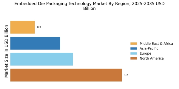
Embedded Die Packaging Technologie Markt Regional Image

Hauptakteure und Wettbewerbseinblicke

The Embedded Die Packaging Technology Market is currently characterized by a dynamic competitive landscape, driven by rapid technological advancements and increasing demand for miniaturization in electronic devices. Major players such as Intel Corporation (US), Samsung Electronics (KR), and TSMC (TW) are at the forefront, each adopting distinct strategies to enhance their market positioning. Intel Corporation (US) focuses on innovation through significant investments in research and development, aiming to lead in advanced packaging technologies. Meanwhile, Samsung Electronics (KR) emphasizes regional expansion and strategic partnerships to bolster its manufacturing capabilities, particularly in Asia. TSMC (TW), on the other hand, is concentrating on optimizing its supply chain and enhancing production efficiency, which collectively shapes a competitive environment that is both collaborative and fiercely competitive.The market structure appears moderately fragmented, with key players employing various business tactics to gain a competitive edge. Localizing manufacturing has become a prevalent strategy, allowing companies to reduce lead times and enhance responsiveness to market demands. Supply chain optimization is also critical, as firms strive to mitigate risks and ensure reliability in their operations. The collective influence of these strategies by major players contributes to a competitive landscape that is increasingly focused on technological innovation and operational efficiency.
In August Intel Corporation (US) announced a groundbreaking partnership with a leading semiconductor materials supplier to develop next-generation embedded die packaging solutions. This collaboration is expected to enhance Intel's capabilities in producing high-performance chips, thereby solidifying its position as a leader in the embedded die packaging sector. The strategic importance of this partnership lies in its potential to accelerate innovation and improve product offerings, catering to the growing demand for advanced semiconductor technologies.
In July Samsung Electronics (KR) unveiled its new embedded die packaging facility in Vietnam, aimed at increasing production capacity and meeting the rising global demand for compact electronic components. This strategic move not only enhances Samsung's manufacturing footprint but also reflects its commitment to regional expansion and supply chain resilience. The establishment of this facility is likely to provide Samsung with a competitive advantage in terms of cost efficiency and production scalability.
In September TSMC (TW) launched a new initiative focused on integrating artificial intelligence into its embedded die packaging processes. This initiative aims to optimize production workflows and enhance quality control through advanced data analytics. The strategic significance of this move is profound, as it positions TSMC at the intersection of AI and semiconductor manufacturing, potentially leading to improved operational efficiencies and product quality.
As of October the competitive trends in the Embedded Die Packaging Technology Market are increasingly defined by digitalization, sustainability, and the integration of AI technologies. Strategic alliances among key players are shaping the landscape, fostering innovation and collaboration. Looking ahead, it is anticipated that competitive differentiation will evolve, shifting from traditional price-based competition to a focus on technological advancements, innovation, and supply chain reliability. This transition underscores the importance of agility and responsiveness in a rapidly changing market.

Zu den wichtigsten Unternehmen im Embedded Die Packaging Technologie Markt-Markt gehören

Recent Industry Developments

  • Q3 2026: Intel Corporation (US): Intel detailed its EMIB and EMIB-T advanced packaging technologies in July 2026, highlighting embedded silicon bridges, chiplet integration, improved power delivery and high-bandwidth memory support for next-generation AI and data-center processors.
  • Q3 2026: Samsung Electronics (KR): Samsung Electronics and Broadcom signed a July 2026 MOU covering advanced packaging built on Samsung’s 2nm process, including 2.3D and 2.5D integration, targeting higher-performance and more power-efficient AI and networking silicon.
  • Q3 2026: TSMC (TW): TSMC expanded its 3DFabric advanced-packaging roadmap in 2026, reporting production of 5.5-reticle CoWoS and plans for a 14-reticle version capable of integrating approximately 10 compute dies and 20 HBM stacks for AI systems
  • Q3 2026: Micron Technology (US): Micron began volume shipments of HBM4 in March 2026 and demonstrated samples of HBM4 48GB 16H using advanced packaging to stack 16 memory dies, increasing capacity per HBM placement for AI computing platforms
  • Q3 2026: STMicroelectronics (FR): STMicroelectronics confirmed continued 2026 investment in next-generation Panel-Level Packaging at its Tours pilot line, alongside back-end capacity expansion and modernization, supporting heterogeneous integration and advanced semiconductor packaging development in Europe
  • Q1 2024: University of Illinois researchers develop new molecular strategies for miniaturized electronic devices In January 2024, scientists at the University of Illinois announced the development of stable, shape-persistent molecules with controlled conductance using a new synthesis method, which could advance the reliability and miniaturization of embedded die packaging technology for electronic devices.

Zukunftsaussichten

Embedded Die Packaging Technologie Markt Zukunftsaussichten

Der Markt für Embedded Die Packaging Technologie ist bereit für ein Wachstum von 7,32 % CAGR von 2024 bis 2035, angetrieben durch Fortschritte in der Miniaturisierung, eine steigende Nachfrage nach leistungsstarker Elektronik und kosteneffizienten Fertigungsprozessen.

Neue Möglichkeiten liegen in:

  • Entwicklung fortschrittlicher thermischer Managementlösungen für eingebettete Die-Pakete.

Bis 2035 wird erwartet, dass der Markt ein robustes Wachstum erzielt und seine Position als Schlüsseltechnologie in der Elektronik festigt.

Marktsegmentierung

Marktanwendungsausblick für Embedded Die Packaging Technologie

  • Verbraucherelektronik
  • Telekommunikation
  • Automobil
  • Industrie

Markt für Embedded Die Packaging Technologie Verpackungsart Ausblick

  • Fan-Out Wafer-Level-Verpackung
  • Eingebettete Wafer-Level-Verpackung
  • 2,5D-Verpackung
  • 3D-Verpackung

Marktübersicht der Materialtypen für Embedded Die Packaging Technologie

  • Silizium
  • Organische Substrate
  • Keramik
  • Polymer

Markt für Embedded Die Packaging Technologie - Ausblick der Endverbraucherindustrie

  • Elektronikfertigung
  • Automobilindustrie
  • Gesundheitsgeräte
  • Luft- und Raumfahrt

Berichtsumfang

MARKTGRÖSSE 2024 2,744 (Milliarden USD)
MARKTGRÖSSE 2025 2,945 (Milliarden USD)
MARKTGRÖSSE 2035 5,969 (Milliarden USD)
DURCHSCHNITTLICHE JÄHRLICHE WACHSTUMSRATE (CAGR) 7,32 % (2024 - 2035)
BERICHTDECKUNG Umsatzprognose, Wettbewerbslandschaft, Wachstumsfaktoren und Trends
GRUNDJAHR 2024
Marktprognosezeitraum 2025 - 2035
Historische Daten 2019 - 2024
Marktprognoseeinheiten Milliarden USD
Profilierte Schlüsselunternehmen Marktanalyse in Bearbeitung
Abgedeckte Segmente Marktsegmentierungsanalyse in Bearbeitung
Schlüsselmarktchancen Fortschritte in der Miniaturisierung und Integration treiben das Wachstum im Markt für Embedded Die Packaging Technologie voran.
Schlüsselmarktdynamiken Die steigende Nachfrage nach Miniaturisierung fördert Innovationen in der Embedded Die Packaging Technologie und verbessert Leistung und Effizienz.
Abgedeckte Länder Nordamerika, Europa, APAC, Südamerika, MEA

Frequently Asked Questions

Was ist die prognostizierte Marktbewertung für den Markt für Embedded Die Packaging Technology im Jahr 2035?
Die prognostizierte Marktbewertung für den Embedded Die Packaging Technology Markt im Jahr 2035 beträgt 5,969 USD Milliarden.
Wie hoch war die Marktbewertung für den Markt für Embedded Die Packaging Technology im Jahr 2024?
Die Marktbewertung für den Embedded Die Packaging Technology Markt im Jahr 2024 betrug 2,744 USD Milliarden.
Was ist die erwartete CAGR für den Markt für Embedded Die Packaging Technologie von 2025 bis 2035?
Die erwartete CAGR für den Markt für Embedded Die Packaging Technology im Prognosezeitraum 2025 - 2035 beträgt 7,32 %.
Welches Anwendungssegment wird bis 2035 voraussichtlich die höchste Bewertung haben?
Das Anwendungssegment der Unterhaltungselektronik wird voraussichtlich bis 2035 1,9 USD Milliarden erreichen.
Was sind die Hauptakteure im Markt für Embedded Die Packaging Technologie?
Wichtige Akteure auf dem Markt sind die Intel Corporation, Samsung Electronics, TSMC und Micron Technology.
Wie ändert sich die Bewertung des Telekommunikationssegments von 2024 bis 2035?
Die Bewertung des Telekommunikationssegments wird voraussichtlich von 0,7 USD Milliarden im Jahr 2024 auf 1,5 USD Milliarden im Jahr 2035 steigen.
Wie hoch ist das prognostizierte Wachstum für das Segment der Automobilanwendungen bis 2035?
Der Automobilanwendungsbereich wird voraussichtlich von 0,6 USD Milliarden im Jahr 2024 auf 1,3 USD Milliarden bis 2035 wachsen.
Welche Verpackungsart wird voraussichtlich den Markt bis 2035 dominieren?
Fan-Out Wafer Level Packaging wird voraussichtlich den Markt dominieren und bis 2035 1,823 USD Milliarden erreichen.
Wie wird das erwartete Wachstum in der Elektronikfertigungs-Endverbraucherindustrie bis 2035 aussehen?
Die Endverbraucherindustrie der Elektronikfertigung wird voraussichtlich von 1,1 USD Milliarden im Jahr 2024 auf 2,5 USD Milliarden bis 2035 wachsen.
Welcher Materialtyp wird voraussichtlich die höchste Bewertung im Jahr 2035 haben?
Silizium wird voraussichtlich die höchste Bewertung erreichen und bis 2035 1,9 USD Milliarden betragen.
Autor
Author Author Profile Aarti Dhapte LinkedIn AVP - Research
A consulting professional focused on helping businesses navigate complex markets through structured research and strategic insights. I partner with clients to solve high-impact business problems across market entry strategy, competitive intelligence, and opportunity assessment. Over the course of my experience, I have led and contributed to 100+ market research and consulting engagements, delivering insights across multiple industries and geographies, and supporting strategic decisions linked to $500M+ market opportunities. My core expertise lies in building robust market sizing, forecasting, and commercial models (top-down and bottom-up), alongside deep-dive competitive and industry analysis. I have played a key role in shaping go-to-market strategies, investment cases, and growth roadmaps, enabling clients to make confident, data-backed decisions in dynamic markets.
Co-Author Co-Author Profile Aarti Dhapte LinkedIn AVP - Research
A consulting professional focused on helping businesses navigate complex markets through structured research and strategic insights. I partner with clients to solve high-impact business problems across market entry strategy, competitive intelligence, and opportunity assessment. Over the course of my experience, I have led and contributed to 100+ market research and consulting engagements, delivering insights across multiple industries and geographies, and supporting strategic decisions linked to $500M+ market opportunities. My core expertise lies in building robust market sizing, forecasting, and commercial models (top-down and bottom-up), alongside deep-dive competitive and industry analysis. I have played a key role in shaping go-to-market strategies, investment cases, and growth roadmaps, enabling clients to make confident, data-backed decisions in dynamic markets.

Research Approach


Secondary Research

The secondary research process involved comprehensive analysis of semiconductor industry databases, peer-reviewed engineering journals, technical publications, and authoritative electronics manufacturing organizations. Key sources included the US Department of Commerce (Bureau of Industry and Security), European Commission (Directorate-General for Internal Market, Industry, Entrepreneurship and SMEs), Semiconductor Industry Association (SIA), Institute of Electrical and Electronics Engineers (IEEE), International Technology Roadmap for Semiconductors (ITRS), SEMI (Semiconductor Equipment and Materials International), IPC (Association Connecting Electronics Industries), National Institute of Standards and Technology (NIST), US Patent and Trademark Office (USPTO), European Patent Office (EPO), World Intellectual Property Organization (WIPO), Organisation for Economic Co-operation and Development (OECD) Science and Technology Indicators, US Census Bureau (Annual Survey of Manufactures), Eurostat (High-Tech Industry Statistics), National Center for Science and Engineering Statistics (NCSES), United Nations Industrial Development Organization (UNIDO), and Ministry of Economy, Trade and Industry (METI) Japan. These sources were used to collect semiconductor production statistics, patent filing data, packaging technology roadmaps, material science research, foundry capacity trends, and market landscape analysis for fan-out wafer level packaging, 2.5D/3D packaging technologies, silicon substrates, organic substrates, and advanced heterogeneous integration solutions.


Primary Research

In order to gather both qualitative and quantitative insights, supply-side and demand-side stakeholders were interviewed during the primary research process. CEOs, VPs of Advanced Packaging, chiefs of R&D, and business unit directors from semiconductor foundries, OSATs (Outsourced Semiconductor Assembly and Test), substrate producers, and providers of packaging equipment were examples of supply-side sources. Demand-side sources included supply chain managers from industrial automation and aerospace firms, procurement chiefs from consumer electronics OEMs, telecommunications equipment makers, and automotive electronics divisions. Market segmentation, technology migration schedules, yield optimization techniques, capital expenditure trends, and supply chain localization dynamics were all confirmed by primary research.

Primary Respondent Breakdown:

By Designation: C-level Primaries (32%), Director Level (30%), Others (38%)

By Region: North America (38%), Europe (25%), Asia-Pacific (32%), Rest of World (5%)


Market Size Estimation

Global market valuation was derived through revenue mapping and wafer/package volume

Kostenloses Muster herunterladen

Bitte füllen Sie das folgende Formular aus, um ein kostenloses Muster dieses Berichts zu erhalten

Download PDF ×

We do not share your information with anyone. However, we may send you emails based on your report interest from time to time. You may contact us at any time to opt-out.