Semiconductor Inspection System Market 摘要
主要市场趋势和亮点
市场规模与预测
| CAGR (2025 - 2035) | 4.45% |
| CAGR (2025 - 2035) | 4.45% |
半导体检测系统市场目前正经历一个变革阶段,受到半导体制造过程复杂性增加的推动。随着技术的进步,对检测系统的精确性和准确性的需求不断上升。该市场的特点是对自动化和人工智能的日益重视,这可能会提高检测过程的效率。此外,先进成像技术的整合变得越来越普遍,表明向更复杂的解决方案转变,以应对更小和更复杂的半导体设计所带来的挑战。此外,半导体检测系统市场似乎受到半导体生产中质量保证需求上升的影响。制造商越来越认识到保持高标准以确保产品可靠性和性能的重要性。这一趋势表明,采用提供实时监控和数据分析能力的检测系统的潜力正在增长。随着行业的发展,利益相关者必须保持警惕并适应不断变化的环境,因为新技术和方法不断涌现,塑造半导体检测的未来。
自动化和人工智能在检测系统中的整合变得越来越普遍。这一趋势表明,制造商正在寻求提高运营效率并减少人为错误,从而提高整体生产力。
在半导体检测系统市场中,先进成像技术的采用正在上升。这一转变表明对高分辨率成像解决方案的需求日益增长,这些解决方案能够有效应对现代半导体设计的复杂性。
在检测系统中,对实时监控和数据分析能力的重视显著。这一趋势反映了行业对质量保证的关注,因为制造商旨在通过持续监督确保产品的可靠性。
The increasing complexity of semiconductor devices is a critical driver for the Semiconductor Inspection System Market. As semiconductor technology evolves, devices are becoming more intricate, with smaller geometries and more layers. This complexity necessitates advanced inspection systems capable of identifying defects that could compromise device performance. Manufacturers are investing in state-of-the-art inspection technologies to address these challenges, ensuring that they can deliver high-quality products. The market for semiconductor inspection systems is expected to expand as companies seek to enhance their production capabilities and maintain compliance with industry standards. This trend highlights the importance of robust inspection processes in the semiconductor manufacturing landscape.
在半导体检测系统市场中,晶圆代表了最大的细分市场,由于其在集成电路和微电子制造中的广泛使用,占据了市场的显著份额。该细分市场的主导地位主要受到对先进半导体设备日益增长的需求的推动,这些设备需要高精度的检测系统来进行晶圆处理。相反,掩模细分市场虽然较小,但正在迅速获得关注,并被认为是市场中增长最快的类别。这一增长反映了光刻工艺在半导体制造中日益重要性,掩模质量直接影响半导体设备的性能。
晶圆(主导)与掩模(新兴)
晶圆被视为半导体检测系统市场中的主导细分市场,其在半导体生产中的重要作用使其具有关键性。它们的关键性在于确保集成电路按照所需规格和质量制造,从而防止可能导致设备故障的缺陷。另一方面,掩模细分市场代表了该市场的新兴方面,受到光刻技术进步的推动,需求激增。随着半导体设计复杂性的增加,对高度准确且无缺陷的掩模的需求变得至关重要,推动了专门针对掩模应用的检测系统的创新。这两个细分市场之间的相互作用突显了半导体制造的不断演变的格局。
在半导体检测系统市场中,市场份额的分布明显倾向于大型企业,由于其显著的资源和成熟的市场存在,持有相当大的份额。该细分市场受益于广泛的财务能力,能够投资于先进的半导体检测技术,确保高质量的生产。另一方面,中小企业正在获得关注,受到对适合其更灵活操作需求的精确检测系统的需求推动,表明市场格局的动态变化。
最终用户:大型企业(主导)与中小企业(新兴)
大型企业在半导体检测系统市场中占主导地位,因其规模、运营能力和投资最新检测技术的能力。它们通常处于创新的前沿,整合复杂的系统以增强质量控制流程,从而确保符合行业标准。相比之下,中小企业(SMEs)通过采用灵活且具有成本效益的检测解决方案,正在成为重要参与者。它们往往优先考虑适应性和效率,而非规模,在需要专门检测应用的细分市场中取得了显著进展,从而推动了该细分市场的增长。
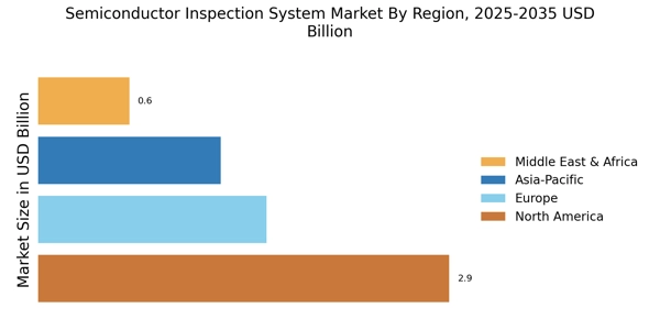
North America is the largest market for semiconductor inspection systems, holding approximately 45% of the global market share. The region's growth is driven by robust demand for advanced semiconductor technologies, fueled by increasing investments in AI, IoT, and automotive sectors. Regulatory support for technology innovation and manufacturing incentives further catalyze market expansion. The United States leads the market, with key players like KLA Corporation, Applied Materials, and Teradyne headquartered here. The competitive landscape is characterized by continuous innovation and strategic partnerships among these companies, ensuring a strong foothold in the global market. The presence of advanced research institutions also bolsters the region's capabilities in semiconductor inspection technologies.
Europe is witnessing significant growth in the semiconductor inspection system market, accounting for around 25% of the global share. The region benefits from strong governmental support for semiconductor initiatives, particularly in countries like Germany and France, which are investing heavily in local manufacturing and R&D. Regulatory frameworks aimed at enhancing technological capabilities are also pivotal in driving market demand. Germany stands out as a leader in the market, with major players like ASML and Nikon Corporation establishing a strong presence. The competitive landscape is evolving, with European companies focusing on innovation and sustainability to meet the growing demand for advanced semiconductor technologies. Collaborative efforts among industry stakeholders are also enhancing the region's market position.
Asia-Pacific is a rapidly growing market for semiconductor inspection systems, holding approximately 20% of the global market share. The region's growth is primarily driven by the increasing demand for consumer electronics and automotive applications, particularly in countries like China, Japan, and South Korea. Government initiatives aimed at boosting semiconductor manufacturing capabilities are also significant growth catalysts. China is the largest market in the region, with substantial investments in semiconductor technology and manufacturing. The competitive landscape features key players like Hitachi High-Technologies and Nikon Corporation, which are focusing on innovation to meet the rising demand. The presence of a robust supply chain and skilled workforce further enhances the region's competitiveness in the semiconductor inspection market.
The Middle East and Africa region is gradually emerging in the semiconductor inspection system market, currently holding about 10% of the global share. The growth is driven by increasing investments in technology and infrastructure, particularly in countries like Israel and South Africa. Government initiatives aimed at fostering innovation and attracting foreign investments are also contributing to market expansion. Israel is a key player in the region, with a focus on advanced semiconductor technologies. The competitive landscape is characterized by a mix of local and international companies, with a growing emphasis on research and development. As the region continues to invest in technology, the semiconductor inspection market is expected to see significant growth in the coming years.
领先的市场公司正在大力投资研发,以增加其产品线,这将进一步推动半导体检测系统市场的增长。重要的市场发展包括新产品发布、合同协议、收购和合并、更多投资以及与其他组织的合作。半导体检测系统行业必须生产具有成本效益的商品,以在竞争日益激烈的市场环境中蓬勃发展。制造商在全球半导体检测系统行业中采用本地生产以降低运营成本是一种有效的商业策略,以服务客户并扩大市场份额。半导体检测系统行业最近提供了一些最重要的好处。KLA Corporation、Kraft Wafers Group Inc.及其他主要竞争者正在通过投资研发活动来提高消费者需求。KLA Corporation是一家总部位于加利福尼亚州米尔皮塔斯的资本设备公司。它为半导体及其他相关纳米电子企业提供工艺控制和产量管理技术。从研发到最终大规模生产,该公司的产品和服务旨在覆盖晶圆、掩模、集成电路(IC)和封装生产的所有阶段。它们结合了全球领导者的规模和更广泛的尖端技术组合,如无图案晶圆质量、3D计量,涵盖从纳米级晶体管到微米级芯片互连、晶圆和封装的宏观缺陷检测、金属互连成分、工厂分析以及用于先进半导体封装的光刻。这一系列的广度使我们能够与客户在从裸硅晶圆到最终后端封装的工艺产量和工艺修改方面进行合作。Onto Innovation的软件为客户提供了更好的了解,帮助他们了解不同操作如何影响整个产品,从而提高产品质量和可靠性。
在12月,KLA Corporation发布了一款新的Axion T2000 X射线计量设备,专为先进内存芯片制造商设计。Axion T2000采用专利方法,以前所未有的分辨率、准确性、精度和速度测量高纵横比设备特性。凭借其在半导体价值链中的独特洞察,Onto Innovation在工艺控制方面独树一帜。他们帮助客户解决最具挑战性的产量、设备性能、质量和可靠性问题。通过使客户变得更聪明、更快、更高效,Onto Innovation将优化其关键的进步路线。Onto Innovation总部位于马萨诸塞州威尔明顿,为客户提供全球销售和服务组织。
在6月,Onto Innovation Inc.,一家排名前三的半导体制造商,获得了配备新EB40模块的Dragonfly G3系统。该系统和模块提供全表面晶圆检测,以解决因晶圆边缘和背面缺陷导致的产量损失,涵盖前端和后端工艺。
Q3 2026: Applied Materials (US): Announced Advantest as an Innovation Partner for its EPIC Center in Silicon Valley, co-locating an Advantest Innovation Center to bridge front-end manufacturing with back-end testing and improve integration of in-line metrology and inspection for AI and 3D advanced packaging.
Q3 2026: Hitachi High-Tech (JP): Launched sales and support activities in India for the FineSAT III ultrasonic inspection system, a non-destructive tool for detecting delamination, voids, and bonding failures in semiconductor packages, supporting quality assurance in India's expanding fab and OSAT ecosystem.
Q3 2026: Teradyne (US): Launched three new UltraFLEXplus instruments including the UltraPort-PCIe6, the industry's first high-speed I/O protocol ATE solution for PCIe Gen6 interfaces, enabling test coverage shifts to earlier insertions for improved Known Good Die confidence.
预计半导体检测系统市场在2025年至2035年间以4.45%的CAGR增长,推动因素包括技术进步、对小型化的需求增加以及严格的质量控制要求。
到2035年,市场预计将实现强劲增长,成为半导体制造中的关键组成部分。
| 市场规模 2024 | 64.01(亿美元) |
| 市场规模 2025 | 66.85(亿美元) |
| 市场规模 2035 | 103.3(亿美元) |
| 年均增长率(CAGR) | 4.45%(2025 - 2035) |
| 报告覆盖范围 | 收入预测、竞争格局、增长因素和趋势 |
| 基准年 | 2024 |
| 市场预测期 | 2025 - 2035 |
| 历史数据 | 2019 - 2024 |
| 市场预测单位 | 亿美元 |
| 关键公司简介 | ASML(荷兰)、KLA Corporation(美国)、应用材料(美国)、尼康公司(日本)、日立高科技公司(日本)、特拉丁(美国)、Rudolph Technologies(美国)、Cohu(美国) |
| 覆盖的细分市场 | 类型、最终用户、地区 |
| 关键市场机会 | 人工智能的进步提高了半导体检测系统市场的精度。 |
| 关键市场动态 | 技术进步推动对复杂半导体检测系统的需求,适应不断变化的行业标准和竞争压力。 |
| 覆盖的国家 | 北美、欧洲、亚太地区、南美、中东和非洲 |
截至2024年,市场估值为64.01亿美元。
预计到2035年,市场估值将达到103.3亿美元。
预计市场在2025年至2035年期间的年均增长率为4.45%。
关键参与者包括ASML、KLA公司、应用材料、尼康公司、日立高科技公司、Teradyne、Rudolph Technologies和Cohu。
市场细分包括晶圆和掩模,预计各自的估值为51.2亿美元和52.1亿美元。
在2024年,中小企业占据了19.2亿美元,而大型企业的市场估值为44.8亿美元。
请填写以下表格以获取本报告的免费样本
“This is really good guys. Excellent work on a tight deadline. I will continue to use you going forward and recommend you to others. Nice job”
“Thanks for sending the report it gives us a good global view of the Betaïne market.”
“We found the report very insightful! we found your research firm very helpful. I'm sending this email to secure our future business.”
“I am very pleased with how market segments have been defined in a relevant way for my purposes (such as "Portable Freezers & refrigerators" and "last-mile"). In general the report is well structured. Thanks very much for your efforts.”
“We got the report in time, we really thank you for your support in this process. I also thank to all of your team as they did a great job.”
“The Automotive 48V ECU Components Procurement Intelligence Study” was a complex project, but the Market Research Future (MRFR) team handled it with quality, agility, and customer-centricity. They delivered all requested data on time and within the agreed scope. The team, including Shubhendra Anand and Rahul Gotadki, was always readily available to clarify questions and swiftly implement necessary adjustments, driving the project to a successful conclusion within a very demanding timeframe.
I would also like to specifically commend Akshay Agarwal for his responsiveness and support at every stage—from our initial inquiry on May 6th through to final delivery on June 18th. His dedication made the entire process seamless.”
“Thanks. It’s been a pleasure working with you, please use me as reference with any other Intel employees.”
“Thank you, this will be very helpful for OQS.”
“I have been reading the first document or the study, ,the Global HVAC and FP market report 2021 till 2026. Must say, good info! I have not gone in depth at all parts, but got a good indication of the data inside!”