Certified Global Research Member
Isomar fd.webp Wcrc 57.webp
Key Questions Answered
  • Global Market Outlook
  • In-depth analysis of global and regional trends
  • Analyze and identify the major players in the market, their market share, key developments, etc.
  • To understand the capability of the major players based on products offered, financials, and strategies.
  • Identify disrupting products, companies, and trends.
  • To identify opportunities in the market.
  • Analyze the key challenges in the market.
  • Analyze the regional penetration of players, products, and services in the market.
  • Comparison of major players financial performance.
  • Evaluate strategies adopted by major players.
  • Recommendations
Why Choose Market Research Future?
  • Vigorous research methodologies for specific market.
  • Knowledge partners across the globe
  • Large network of partner consultants.
  • Ever-increasing/ Escalating data base with quarterly monitoring of various markets
  • Trusted by fortune 500 companies/startups/ universities/organizations
  • Large database of 5000+ markets reports.
  • Effective and prompt pre- and post-sales support.

Wafer Inspection System Market Research Report Information By Technology (E-Beam Detection Technology and Optical Detection Technology), By Defect Type (Random Defects Detection and Systematic Defects Detection) And By Region (North America, Europe, Asia-Pacific, And Rest Of The World) โ€“Market Forecast Till 2032


ID: MRFR/SEM/15651-HCR | 128 Pages | Author: Aarti Dhapte| April 2024

Global Wafer Inspection System Market Overview


Wafer Inspection System Market Size was valued at USD 3.8 Billion in 2022. The Wafer Inspection System market industry is projected to grow from USD 4.218 Billion in 2023 to USD 9.720 Billion by 2032, exhibiting a compound yearly growth rate (CAGR) of 11.00% during the forecast period (2023 - 2032). Increased demand for higher semiconductor manufacturing yields and the need for advanced quality control in the production of integrated circuits are the key market drivers enhancing market growth.


Wafer Inspection System Market Overview


Source: The Secondary Research, Primary Research, MRFR Database and Analyst Review


Wafer Inspection System Market Trends


  • Growing demand for higher semiconductor manufacturing yields is driving the market growth


Market CAGR for wafer inspection systems is being driven by the rising demand for higher semiconductor manufacturing yields. As semiconductor technology continues to advance, there is an increasing need for greater precision and reliability in the manufacturing process. Higher yields, which refer to the percentage of usable and defect-free semiconductor components on a wafer, are crucial for maximizing the efficiency and profitability of semiconductor fabrication.


Wafer inspection systems play an important role in meeting this demand by providing a comprehensive and automated means of detecting defects and irregularities at various stages of semiconductor production. These systems employ advanced imaging, sensing, and analysis technologies to scrutinize the surface and critical layers of semiconductor wafers, identifying even minute imperfections that could compromise the functionality or reliability of the final products. Achieving and maintaining high yields is essential for semiconductor manufacturers to reduce production costs and enhance overall profitability. By integrating wafer inspection systems into the manufacturing process, semiconductor companies can identify and address defects early, preventing the production of faulty components and minimizing waste. This proactive approach not only enhances the overall yield but also contributes to the production of high-quality semiconductor devices that meet the stringent requirements of modern electronic applications.


Furthermore, as semiconductor devices become smaller and more complex, the importance of precise defect detection increases. Wafer inspection systems are designed to handle the challenges posed by advanced semiconductor manufacturing technologies, including those associated with smaller node sizes, 3D structures, and new materials. The continuous evolution of wafer inspection technologies is closely aligned with the industry's pursuit of higher yields, making these systems indispensable for maintaining the competitiveness and efficiency of semiconductor manufacturing on a global scale. Further, the growing complexity of semiconductor designs, including three-dimensional structures and intricate patterns, makes it more challenging to identify defects using traditional inspection methods. Wafer inspection systems use advanced imaging and sensing technologies, such as optical and electron microscopy, to provide detailed and high-resolution views of the wafer's surface, enabling precise defect detection in complex structures.


Early detection and correction of defects with wafer inspection systems help in minimizing production costs. By preventing the manufacture of defective or low-quality chips, manufacturers can avoid unnecessary material and labor expenses associated with producing components that may not meet quality standards. This cost-effectiveness is a significant driver for the adoption of wafer inspection systems. Thus driving the Wafer Inspection System market revenue.


Wafer Inspection System Market Segment Insights


Wafer Inspection System Technology Insights


The Wafer Inspection System Market segmentation, based on technology, includes E-Beam Detection Technology and Optical Detection Technology. The e-beam detection technology segment dominated the market, accounting for the largest market revenue due to its unparalleled precision and ability to detect extremely small defects on semiconductor wafers. E-beam inspection provides high-resolution imaging at the nanoscale, enabling the identification of subtle deviations and defects that other inspection methods might miss. This level of sensitivity is crucial as semiconductor manufacturing processes continue to produce chips with increasingly smaller feature sizes. The demand for e-beam detection technology is further driven by its capacity to inspect advanced integrated circuit designs, making it a preferred choice for semiconductor manufacturers seeking comprehensive and reliable quality control in their production processes. Optical Detection Technology is the fastest-growing segment of the wafer inspection market due to the increasing demand for high-throughput inspection systems.


Wafer Inspection System Defect Type Insights


The Wafer Inspection System Market segmentation, based on defect type, includes Random Defects Detection and Systematic Defects Detection. The random defects detection category dominates the market due to its important role in ensuring the reliability and functionality of integrated circuits. As semiconductor manufacturing processes advance, the likelihood of random defects, such as particles or anomalies, affecting the final product increases. Wafer inspection systems equipped with advanced technologies for random defect detection, such as high-resolution imaging and sophisticated algorithms, are essential for identifying and characterizing these unpredictable imperfections. The ability to swiftly and accurately detect random defects is a key factor in maintaining high yields, minimizing production costs, and upholding the stringent quality standards demanded by the semiconductor industry.


Figure 1: Wafer Inspection System Market, by Defect Type, 2022 & 2032 (USD Billion)


Wafer Inspection System Market, by Defect Type, 2022 & 2032


Source: The Secondary Research, Primary Research, MRFR Database and Analyst Review


Wafer Inspection System Regional Insights


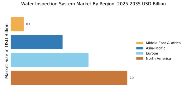
By region, the study gives market insights into the North America, Europe, Asia-Pacific, and the Rest of the World. The North American Wafer Inspection System market area dominates this market due to its strong presence of leading semiconductor manufacturers and a robust ecosystem of technology and innovation. The region's leadership in semiconductor research and development, coupled with a high demand for advanced electronics across industries, positions North America as a key hub for the adoption and advancement of wafer inspection technologies.


Further, the major countries studied in the market report are The US, Canada, Germany, France, the UK, Italy, Spain, Japan, China, India, Australia, South Korea, and Brazil.


Figure 2: WAFER INSPECTION SYSTEM MARKET SHARE BY REGION 2022 (USD Billion)


WAFER INSPECTION SYSTEM MARKET SHARE BY REGION 2022


Source: The Secondary Research, Primary Research, MRFR Database and Analyst Review


Europe's Wafer Inspection System market accounts for the second-largest market share due to the region's emphasis on precision manufacturing, technological innovation, and the demand for high-quality semiconductor products in industries. Further, the German Wafer Inspection System market held the largest market share, and the UK Wafer Inspection System market was the fastest-growing market in the European region.


The Asia-Pacific Wafer Inspection System Market is foreseen to grow at the fastest CAGR from the year 2023 to 2032. This is due to the region's significant role as a global semiconductor manufacturing hub, with increasing investments in technology, rising demand for consumer electronics, and a burgeoning semiconductor industry. Moreover, China’s Wafer Inspection System market held the largest market share, and the Indian Wafer Inspection System market was the fastest-growing market in the Asia-Pacific region.


Wafer Inspection System Key Market Players & Competitive Insights


Leading market players are investing heavily in the research and development in order to expand their product lines, which will help the Wafer Inspection System market grow even more. Market players  are also undertaking a variety of strategic activities to spread their global footprint, with important market developments including mergers and acquisitions, new product launches, contractual agreements, higher investments, and collaboration with other organizations. To spread and survive in a more competitive and rising market climate, the Wafer Inspection System industry must offer cost-effective items.


Manufacturing locally to minimize the operational costs is one of the key business tactics used by the manufacturers in the global Wafer Inspection System industry to benefit the clients and increase the market sector. In recent years, the Wafer Inspection System industry has offered some of the most significant advantages to different industries. Major players in the Wafer Inspection System market, including Applied Materials, Inc., KLA-Tencor Corporation, ASML Pacific Technology, Teradyne Inc., Nanda Technologies GmBH, Lam Research Corporation, Hitachi High-Technologies Corporation, Hermes Microvision, Inc., NXP Semiconductors, Synopsys, and others, are trying to increase market demand by investing in the research and development operations.


KLA Corporation is a renowned global leader in advanced process control and attain management solutions for the semiconductor and related industries. Headquartered in Milpitas, California, the company plays a pivotal role in enabling the high performance and reliability of electronic devices by providing innovative technologies for process diagnostics, inspection, metrology, and data analytics. With a strong focus on semiconductor manufacturing, KLA Corporation's comprehensive portfolio of products and services caters to various critical stages of the semiconductor fabrication process. In October 2023, KLA Corporation, a leading provider of process inspection and control technologies for the semiconductor and microelectronics industries, acquired Cohu, Inc., a provider of semiconductor capital equipment and services, for $6.45 billion. This acquisition is expected to expand KLA's product portfolio and provide it with access to new markets.


ASML Holding NV is a Dutch multinational company and a global leader in the development and manufacturing of photolithography equipment used in semiconductor manufacturing. Headquartered in Veldhoven, Netherlands, ASML specializes in producing advanced lithography machines that play a pivotal role in the fabrication of integrated circuits and microchips. The company's cutting-edge Extreme Ultraviolet (EUV) lithography technology is particularly noteworthy, enabling the production of smaller and more powerful semiconductor components. In September 2023, ASML Holding NV, a Dutch manufacturer of semiconductor manufacturing equipment, acquired Lam Research Corporation, a U.S. manufacturer of semiconductor etching and deposition equipment, for $39 billion. This acquisition is expected to create the world's largest supplier of semiconductor manufacturing equipment.


Key Companies in the Wafer Inspection System market include


  • Applied Materials, Inc.

  • KLA-Tencor Corporation

  • ASML Pacific Technology

  • Teradyne Inc.

  • Nanda Technologies GmBH

  • Lam Research Corporation

  • Hitachi High-Technologies Corporation

  • Hermes Microvision, Inc.

  • NXP Semiconductors

  • Synopsys


Wafer Inspection System Industry Developments


August 2023: Teradyne Inc., a U.S. manufacturer of semiconductor test equipment, acquired Universal Instruments Corporation, a U.S. manufacturer of semiconductor test equipment, for $2.5 billion. This acquisition is expected to create a leader in the semiconductor test equipment market.


August 2023: ASM Pacific Technology, a Dutch manufacturer of semiconductor equipment, acquired Coventor, a US manufacturer of wafer inspection systems, for USD 4.9 billion. This acquisition will help ASM Pacific Technology to expand its product portfolio and become a leading provider of wafer inspection solutions.


June 2023: Applied Materials, a U.S.-based supplier of semiconductor materials and equipment, acquired Coventor, a U.S.-based provider of optical inspection and metrology solutions, for $1.05 billion. The acquisition is expected to expand Applied Materials' product portfolio and strengthen its position in the wafer inspection market.


Wafer Inspection System Market Segmentation


Wafer Inspection System Technology Outlook


  • E-Beam Detection Technology

  • Optical Detection Technology


Wafer Inspection System Defect Type Outlook


  • Random Defects Detection

  • Systematic Defects Detection


Wafer Inspection System Regional Outlook


  • North America

    • US

    • Canada


  • Europe

    • Germany

    • France

    • UK

    • Italy

    • Spain

    • Rest of Europe


  • Asia-Pacific

    • China

    • Japan

    • India

    • Australia

    • South Korea

    • Australia

    • Rest of Asia-Pacific


  • Rest of the World

    • Middle East

    • Africa

    • Latin America


Report Attribute/Metric Details
Market Size 2022 USD 3.8 Billion
Market Size 2023 USD 4.2218 Billion
Market Size 2032 USD 9.720 Billion
Compound Annual Growth Rate (CAGR) 11.00% (2023-2032)
Base Year 2022
Market Forecast Period 2023-2032
Historical Data 2018- 2022
Market Forecast Units Value (USD Billion)
Report Coverage Revenue Forecast, The Market Competitive Landscape, Growth Factors, and Trends
Segments Covered Technology, Defect Type, and Region
Geographies Covered North America, Europe, Asia Pacific, and the Rest of the World
Countries Covered The US, Canada, Germany, France, UK, Italy, Spain, Japan, China, India, Australia, South Korea, and Brazil
Key Companies Profiled Applied Materials, Inc., KLA-Tencor Corporation, ASML Pacific Technology, Teradyne Inc., Nanda Technologies GmBH, Lam Research Corporation, Hitachi High-Technologies Corporation, Hermes Microvision, Inc., NXP Semiconductors, Synopsys
Key Market Opportunities The need for advanced quality control in the production of integrated circuits.
Key Market Dynamics Increased demand for higher semiconductor manufacturing yields.


Frequently Asked Questions (FAQ) :

The Wafer Inspection System Market size was valued at USD 3.8 Billion in 2022.

The global market is foreseen to rise at a CAGR of 11.00% during the forecast period, 2023-2032.

North America had the largest share of the global market

The key players in the market are Applied Materials, Inc., KLA-Tencor Corporation, ASML Pacific Technology, Teradyne Inc., Nanda Technologies GmBH, Lam Research Corporation, Hitachi High-Technologies Corporation, Hermes Microvision, Inc., NXP Semiconductors, Synopsys.

The E-Beam Detection Technology category dominated the market in 2022.

The Random Defects Detection had the largest share in the global market.

Leading companies partner with us for data-driven Insights
client_1 client_2 client_3 client_4 client_5 client_6 client_7 client_8 client_9 client_10
Kindly complete the form below to receive a free sample of this Report
Please fill in Business Email for Quick Response

We do not share your information with anyone. However, we may send you emails based on your report interest from time to time. You may contact us at any time to opt-out.

Purchase Option
Single User $ 4,950
Multiuser License $ 5,950
Enterprise User $ 7,250
Compare Licenses
Tailored for You
  • Dedicated Research on any specifics segment or region.
  • Focused Research on specific players in the market.
  • Custom Report based only on your requirements.
  • Flexibility to add or subtract any chapter in the study.
  • Historic data from 2014 and forecasts outlook till 2040.
  • Flexibility of providing data/insights in formats (PDF, PPT, Excel).
  • Provide cross segmentation in applicable scenario/markets.