ID: MRFR/SEM/6929-HCR | 111 Pages | Published By Ankit Gupta on April 2023
The Global Wafer Fabrication Market is expected to grow at USD 102.4 Billion by 2030, at a CAGR of 5.20% during the forecast period.
$102.4 Billion
5.20%
Asia Pacific
2022-2030
The global wafer fabrication market share is projected to register a CAGR of 5.20% from 2022 to 2030. Electrical circuits are made through a process called wafer fabrication. Radiofrequency amplifiers, LEDs, and optical computers are all components of photonic production. The technique converts the unfinished wafers into finished chips. Each electrical structure through this component has a different process. Semiconductor wafer fabrication is necessary for the conductors, resistors, and transistors. The wafer fabrication market size is expected to reach approximately USD 102.4 billion by 2030. The industries with the greatest need for integrated circuits are manufacturing facilities. As a result, the market for wafer fabrication is consistently growing in demand. Both electronic and non-electronic devices employ the circuits that the component creates.
The Covid-19 pandemic impacted various industries' daily operations. The demand for wafer fabrication is increasing as interest in hybrid vehicles grows. Due to the pandemic, there were uncertainties in the worldwide wafer fabrication industry. The virus's proliferation has caused severe supply chain problems for the market. The decrease in semiconductor wafer shipments has impacted the price of the product. In this market, China is a major player.
Additionally, it is a region where the virus first appeared. Since 2020, the market has experienced numerous changes. A scarcity of raw materials, limited production, and decreased demand are the results of these problems. Strict government oversight made things much more difficult in the market.
These wafers are used extensively in portable medical equipment in particular. This trend is causing the market's demand to rise steadily. Additionally, the use of wafer fabrication is increasing due to the expansion of the telecom industry. There are numerous applications for this device. The telecom industry's technological improvements encourage greater use of wafer fabrication.
Front-end semiconductor production facilities, or fabs, have recently operated above 80% capacity utilization, with some fabs running as high as 90-100% due to the rising demand for semiconductors. However, because it takes so long to manufacture semiconductors, their capacity utilization must be increased. Due to the worldwide chip scarcity, the semiconductor industry is rapidly expanding fab capacity utilization to satisfy the rising demand. Semiconductor manufacturers launched 19 new high-volume fabs in 2021, and another 10 high-volume fabs are expected to be built in 2022, according to SEMI's World Fab Forecast, published in June 2021.
To fabricate semiconductors, a clean space and clean tools are necessary. Small dust particles can significantly harm the company's bottom line by interfering with the manufacturing system as a whole. Order cancellations and customer switching to other suppliers result in extra losses due to the delivery delay brought on by manufacturing flaws. Common semiconductor flaws include those related to the raw material(s) utilized, the structural integrity, and chip circuitry. Innovative fabrication methods are necessary for the semiconductor manufacturing process to manufacture high-quality semiconductors. The existence of several patterns on a chip at a very small scale, which necessitates great accuracy for sending precise data to the chip, causes an increase in pattern complexity. The ongoing push to make semiconductor devices smaller and denser has increased the complexity of wafers, which in turn reduces the lithography wavelength. Due to the increased complexity of photomasks and wafers brought on by the reduction in node size, new semiconductor manufacturing machinery would be required. All of these problems limit the market's expansion for the market.
Governments worldwide have made the strategic relevance of semiconductors and their growing importance for economic competitiveness and supply chain resilience a top concern. All end-user industries, including the automotive and consumer electronics sectors, are extremely concerned about supply chain disruptions and the chip shortage. Increased geopolitical unrest has highlighted the necessity for some nations to realign and strengthen their positions within the semiconductor supply chain. Different governments have been investigating and developing different plans for the domestic expansion of the semiconductor industry.
Based on the size, the wafer fabrication market segmentation is 65 nm, 45 nm, 32 nm, 22 nm,14 nm, 10 nm, and 7nm. The wafer fabrication market growth was prominently high under the 65 nm category in 2021 due to the growing need for larger memory storage capacities in electronic devices. However, 32 nm is anticipated to be the fastest growing in the coming years as the telecom industry is growing.
Based on the fabrication process, the wafer fabrication market segmentation is front-end of line processing and back-end of line processing. In 2021, the front-end of line processing accounted for the largest market share of the market. The front-end of line processing ensures that the circuit's numerous parts, such as the resistors, transistors, and capacitors, are integrated. However, the back end of the line processing category is estimated to register the highest growth rate during the forecast period. The BOEL ensures the interconnection of the various electrical components on the wafer, whereas with the wafer.
The market is divided into memory manufacturer and integrated device manufacturer based on material. The memory manufacturer category dominated the wafer fabrication industry in 2021. Due to the growing popularity of electric and driverless vehicles, the automotive industry is expected to use memory-integrated circuits (ICs) more frequently. The integrated device manufacturer category is anticipated to witness significant growth over the forecast period. A semiconductor business, an integrated device manufacturer (IDM), creates, produces, and markets integrated circuit (IC) goods. When a business manages semiconductor manufacturing internally, it is referred to as an IDM instead of a fabless semiconductor company, which outsources production to a different semiconductor fabrication facility.
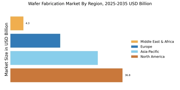
By region, the wafer fabrication market has been divided into North America, Europe, Asia-Pacific, and the Rest of the World. Asia-Pacific accounted for the most extensive market share. Europe will exhibit the highest CAGR during the forecast period.
Asia-Pacific
Asia-Pacific dominated the market share in 2021. Because high-speed internet is becoming more widely used in Asia-Pacific nations, urbanization is growing, and labor costs are rising, which is growing the market. Additionally, the need for wafer fabrication in China is increasing due to the integrated circuit. Japan and China have made significant contributions to the market's rapid expansion. China is the largest producer of semiconductors in the world and the largest consumer of chips. For instance, the Semiconductor Industry Association (SIA) projects that the Chinese semiconductor industry would invest between US$12.3 billion and US$15.3 billion between 2021 and 2022, with CAPEX accounting for roughly 15% of the total worldwide investment.
North America
North America accounted for the second-largest market share in 2021. The market is supported by the rising demand for and widespread use of consumer electronics products in the area. The adoption of the wafer fabrication technique in this region's electronic device production has been encouraged by rapidly evolving technology. The market size is also positively impacted by significant regional technological players like Lam Research, Motorola Solutions, and Applied Materials.
The participants are focusing their efforts on promoting R&D. Additionally, they embrace strategic growth activities to improve their market position and expand their consumer bases, such as product introduction, joint ventures, and partnerships. For instance, in December 2022, tata began the production of semiconductors.
Prominent players in the wafer fabrication market research include Tokyo Electron Limited, KLA-Tencor Corporation, ASML Holding NV, Lam Research Corporation, Intel Corporation, Motorola Solutions Inc, SCREEN Semiconductor Solutions Co. Ltd, Applied Materials Inc, Hitachi High-Technologies Corporation, Samsung, among others.
The objectives of the study are summarized in 5 stages. They are as mentioned below:
To identify and estimate the market size for the wafer fabrication market report segmented by size, fabrication process, and end user by value (in US dollars). Also, to understand the consumption/ demand created by consumers in the wafer fabrication market forecast between 2022 and 2030
To identify and infer the drivers, restraints, opportunities, and challenges in the wafer fabrication market growth
To find out the factors which are affecting the wafer fabrication market size among consumers
To identify and understand the various factors involved in the market affected by the pandemic
To provide a detailed insight into the major companies operating in the market. The profiling will include the financial health of the company in the past 2-3 years with segmental and regional revenue breakup, product offering, recent developments, market statistics, SWOT analysis, and key strategies.
Report Attribute/Metric | Details |
Market Size 2030 | USD 102.4 Billion |
Compound Annual Growth Rate (CAGR) | 5.20%Â (2022-2030) |
Base Year | 2021 |
Market Forecast Period | 2022-2030 |
Historical Data | 2018 & 2020 |
Market Forecast Units | Value (USD Billion) |
Report Coverage | Revenue Forecast, Market Competitive Landscape, Growth Factors, and Trends |
Segments Covered | Size, Fabrication Process, and End User |
Geographies Covered | North America, Europe, Asia Pacific, and Rest of the World |
Countries Covered | The U.S, Canada, Germany, France, UK, Italy, Spain, China, Japan, India, Australia, South Korea, and Brazil |
Key Companies Profiled | Tokyo Electron Limited, KLA-Tencor Corporation, ASML Holding NV, Lam Research Corporation, Intel Corporation, Motorola Solutions Inc, SCREEN Semiconductor Solutions Co. Ltd, Applied Materials Inc, Hitachi High-Technologies Corporation, Samsung |
Key Market Opportunities | Initiatives by the government to support the semiconductor industry |
Key Market Dynamics | An increase in the rising need for semiconductor manufacturing facilities |
The segments of the market, by equipment type, are diffusion systems, oxidation systems, epitaxial reactors, ion implantation equipment, photolithography equipment, and others.
The wafer fabrication market forecast period is 2022 - 2030
The market is expected to register a CAGR of ~5.20% over the next 10 years, according to wafer fabrication market research.
North America is expected to register the highest CAGR during 2022 - 2030
Asia-Pacific held the largest share in 2021
The market size is expected to be USD 102.4 billion by 2030.
Tokyo Electron Limited, KLA-Tencor Corporation, ASML Holding NV, Lam Research Corporation, Intel Corporation, Motorola Solutions Inc, SCREEN Semiconductor Solutions Co. Ltd, Applied Materials Inc, Hitachi High-Technologies Corporation, and Samsung, among others are the major companies operating in the market.