• Cat-intel
  • MedIntelliX
  • Resources
  • About Us
  • Request Free Sample ×

    Kindly complete the form below to receive a free sample of this Report

    Leading companies partner with us for data-driven Insights

    clients tt-cursor
    Hero Background

    Fan Out Wafer Level Packaging Market

    ID: MRFR/PNT/22668-HCR
    111 Pages
    Snehal Singh
    October 2025

    Fan Out Wafer Level Packaging Market Research Report By Wafer Diameter (200 mm, 300 mm), By Product Type (Fan-Out Panel-Level Packaging (FOPLP), Fan-Out in Laminate (FOIL), Embedded Die Fan-Out Wafer Level Packaging (eDFOWLP)), By Substrate Material (Glass, Polymer, Interposer), By Application (Smartphones, Tablets, Automotive, Wearables, Artificial Intelligence (AI) and Machine Learning (ML)) and By Regional (North America, Europe, South America, Asia Pacific, Middle East and Africa) - Forecast to 2035

    Share:
    Download PDF ×

    We do not share your information with anyone. However, we may send you emails based on your report interest from time to time. You may contact us at any time to opt-out.

    Fan Out Wafer Level Packaging Market Infographic

    Fan Out Wafer Level Packaging Market Summary

    As per MRFR analysis, the Fan Out Wafer Level Packaging Market was estimated at 17.52 USD Billion in 2024. The Fan Out Wafer Level Packaging industry is projected to grow from 18.69 USD Billion in 2025 to 35.62 USD Billion by 2035, exhibiting a compound annual growth rate (CAGR) of 6.66 during the forecast period 2025 - 2035.

    Key Market Trends & Highlights

    The Fan Out Wafer Level Packaging Market is poised for substantial growth driven by technological advancements and increasing demand for miniaturization.

    • The market is experiencing a rising demand for miniaturization, particularly in high-performance electronics.
    • North America remains the largest market, while Asia-Pacific is recognized as the fastest-growing region in this sector.
    • In terms of segments, 300 mm technology dominates the market, whereas 200 mm is emerging as the fastest-growing segment.
    • Key drivers include the increasing adoption of IoT devices and the growing demand for high-performance electronics, which are shaping market dynamics.

    Market Size & Forecast

    2024 Market Size 17.52 (USD Billion)
    2035 Market Size 35.62 (USD Billion)
    CAGR (2025 - 2035) 6.66%

    Major Players

    Taiwan Semiconductor Manufacturing Company (TW), Samsung Electronics (KR), Intel Corporation (US), STMicroelectronics (FR), ASE Technology Holding Co., Ltd. (TW), Amkor Technology, Inc. (US), NXP Semiconductors (NL), Texas Instruments (US), Qualcomm Technologies, Inc. (US)

    Fan Out Wafer Level Packaging Market Trends

    The Fan Out Wafer Level Packaging Market is currently experiencing a transformative phase, driven by the increasing demand for miniaturization and enhanced performance in electronic devices. This market segment appears to be gaining traction due to its ability to provide a compact form factor while maintaining high functionality. As industries such as consumer electronics, automotive, and telecommunications continue to evolve, the need for advanced packaging solutions becomes more pronounced. The integration of Fan Out Wafer Level Packaging technology is likely to facilitate the development of next-generation products, which may include smartphones, wearables, and IoT devices. Moreover, the market seems to be influenced by the growing emphasis on energy efficiency and thermal management. Manufacturers are exploring innovative materials and processes to optimize performance while reducing power consumption. This trend indicates a shift towards sustainable practices within the semiconductor industry, as companies strive to meet regulatory standards and consumer expectations. As the Fan Out Wafer Level Packaging Market progresses, it may witness further advancements in design and manufacturing techniques, potentially leading to enhanced reliability and cost-effectiveness in the long run.

    Rising Demand for Miniaturization

    The trend towards miniaturization in electronic devices is propelling the Fan Out Wafer Level Packaging Market. As consumers seek smaller, more powerful gadgets, manufacturers are increasingly adopting this packaging technology to meet these demands.

    Focus on Energy Efficiency

    There is a growing emphasis on energy efficiency within the Fan Out Wafer Level Packaging Market. Companies are investing in innovative materials and processes that not only enhance performance but also reduce power consumption.

    Advancements in Manufacturing Techniques

    The market is witnessing advancements in manufacturing techniques that aim to improve the reliability and cost-effectiveness of Fan Out Wafer Level Packaging. These innovations may lead to more efficient production processes and better product performance.

    The evolution of the Global Fan Out Wafer Level Packaging Market appears to be driven by the increasing demand for miniaturization and enhanced performance in semiconductor devices, suggesting a transformative shift in packaging technologies.

    U.S. Department of Commerce

    Fan Out Wafer Level Packaging Market Drivers

    Increasing Adoption of IoT Devices

    The proliferation of Internet of Things (IoT) devices is a key driver for the Fan Out Wafer Level Packaging Market. As more devices become interconnected, the demand for compact and efficient packaging solutions rises. Fan Out Wafer Level Packaging (FOWLP) offers a smaller footprint, which is essential for IoT applications where space is limited. According to recent estimates, the number of connected IoT devices is expected to reach over 30 billion by 2030. This surge in IoT adoption necessitates advanced packaging technologies that can support high-density interconnections while maintaining performance. Consequently, the Fan Out Wafer Level Packaging Market is likely to experience substantial growth as manufacturers seek to meet the requirements of this expanding market.

    Advancements in Semiconductor Technology

    The rapid advancements in semiconductor technology are a pivotal driver for the Fan Out Wafer Level Packaging Market. Innovations in chip design and fabrication techniques are enabling the development of smaller, more powerful semiconductors. FOWLP is particularly well-suited for these advanced chips, as it allows for higher integration levels and improved electrical performance. The semiconductor market is projected to reach a valuation of over 600 billion by 2025, indicating a robust demand for advanced packaging solutions. As semiconductor manufacturers continue to push the boundaries of technology, the Fan Out Wafer Level Packaging Market is likely to benefit from the increasing need for efficient and effective packaging solutions.

    Rising Focus on Thermal Management Solutions

    Thermal management is becoming increasingly crucial in the electronics industry, driving the Fan Out Wafer Level Packaging Market. As devices become more powerful, effective heat dissipation is essential to ensure reliability and performance. FOWLP technology offers superior thermal performance compared to traditional packaging methods, making it an attractive option for manufacturers. The market for thermal management solutions is expected to witness significant growth, with estimates suggesting a value exceeding 5 billion by 2026. This growing emphasis on thermal efficiency is likely to propel the adoption of Fan Out Wafer Level Packaging, as it provides enhanced thermal conductivity and reliability, thereby addressing the challenges posed by high-performance applications.

    Emerging Applications in Automotive Electronics

    The emergence of advanced automotive electronics is significantly impacting the Fan Out Wafer Level Packaging Market. With the rise of electric vehicles and autonomous driving technologies, there is a growing need for sophisticated electronic systems that require efficient packaging solutions. FOWLP provides the necessary integration and miniaturization capabilities to support these complex applications. The automotive electronics market is anticipated to grow at a compound annual growth rate of approximately 7% over the next few years. This growth presents a substantial opportunity for the Fan Out Wafer Level Packaging Market, as manufacturers seek to leverage advanced packaging technologies to enhance the performance and reliability of automotive electronic systems.

    Growing Demand for High-Performance Electronics

    The increasing demand for high-performance electronics is significantly influencing the Fan Out Wafer Level Packaging Market. As consumer electronics evolve, there is a pressing need for packaging solutions that can accommodate advanced functionalities without compromising on size or efficiency. FOWLP technology enables the integration of multiple components into a single package, enhancing performance while reducing overall dimensions. The market for high-performance electronics, including smartphones and tablets, is projected to grow at a compound annual growth rate of over 6% in the coming years. This trend underscores the necessity for innovative packaging solutions, positioning the Fan Out Wafer Level Packaging Market as a critical player in meeting these evolving demands.

    Market Segment Insights

    By Wafer Diameter: 300 mm (Largest) vs. 200 mm (Fastest-Growing)

    In the Fan Out Wafer Level Packaging Market, the wafer diameter segment exhibits significant variation in market share. The 300 mm wafer diameter is the largest segment, primarily due to its widespread adoption in high-performance applications such as smartphones and computing devices. This size is favored for its ability to enhance manufacturing efficiency and integration density. Meanwhile, the 200 mm wafer diameter, while smaller, is witnessing rapid growth as it finds increasing applications in automotive electronics and IoT devices, catering to the rising demand for smaller, more efficient components. Growth trends in the wafer diameter segment reveal a dynamic landscape driven by technological advancements and market demands. The 300 mm wafer size continues to thrive, supported by advancements in semiconductor technologies that enhance packaging efficiency and performance. Conversely, the 200 mm segment is emerging as a strong contender, fueled by the surge in demand for low-cost, high-efficiency packaging solutions that cater to a broader array of applications in the electronics market, including consumer goods and industrial devices.

    Wafer Diameter: 300 mm (Dominant) vs. 200 mm (Emerging)

    The 300 mm wafer diameter stands as the dominant force in the Fan Out Wafer Level Packaging Market, celebrated for its superior yield, scalability, and integration capabilities, which make it ideal for high-volume manufacturing. This wafer size is particularly well-suited for advanced applications, such as high-performance computing and mobile devices, where performance density is paramount. On the other hand, the 200 mm wafer diameter is emerging as a notable player, gaining traction due to its lower production costs and suitability for less complex designs. It serves a growing demand within automotive and Internet of Things (IoT) markets, where manufacturers are seeking efficient, cost-effective solutions that align with evolving technology trends.

    By Product Type: Fan-Out Panel-Level Packaging (Largest) vs. Embedded Die Fan-Out Wafer Level Packaging (Fastest-Growing)

    The Fan Out Wafer Level Packaging market shows a diverse distribution of segments among its product types. Fan-Out Panel-Level Packaging (FOPLP) currently leads the market, accounting for the largest share due to its advanced manufacturing process that offers higher performance and scalability. On the other hand, Embedded Die Fan-Out Wafer Level Packaging (eDFOWLP) is gaining momentum, attracting significant attention for its ability to integrate multiple functionalities efficiently. This changing dynamic hints at a robust competition across these segments. As technology advances, the demand for innovative packaging solutions continues to rise. The increased adoption of smartphones and various consumer electronics has propelled the growth of the Fan-Out in Laminate (FOIL) and eDFOWLP segments. The shift towards smaller and more efficient packaging methods, along with technological advancements such as enhanced thermal performance and reduced form factors, are key drivers propelling eDFOWLP growth, establishing it as a vital player in the future market landscape.

    Fan-Out Panel-Level Packaging (Dominant) vs. Fan-Out in Laminate (Emerging)

    Fan-Out Panel-Level Packaging (FOPLP) stands out as the dominant force in the Fan Out Wafer Level Packaging market, recognized for its capability to deliver high-density interconnections and superior performance characteristics. Its robust architecture provides significant advantages in terms of thermal performance and electrical efficiency, making it a preferred choice among manufacturers aiming to meet the increasing demands for advanced packaging solutions. In contrast, Fan-Out in Laminate (FOIL) is emerging as a promising alternative, attracting interest for its cost-efficiency and versatility. FOIL technology offers the potential for larger package sizes and integration of diverse semiconductor devices, positioning it uniquely in various applications. With ongoing innovations, FOIL is set to challenge established norms, creating a competitive environment where both segments can flourish.

    By Substrate Material: Glass (Largest) vs. Polymer (Fastest-Growing)

    In the Fan Out Wafer Level Packaging Market, the distribution of substrate materials reveals a significant preference for glass substrates, which take the lead in market share due to their superior performance characteristics such as thermal stability and reliability. In contrast, polymers are gaining traction, especially in emerging applications, and are currently recognized as the fastest-growing segment owing to their lightweight and cost-effective properties that appeal to manufacturers of consumer electronics and advanced packaging solutions.

    Substrate Material: Glass (Dominant) vs. Polymer (Emerging)

    Glass substrates are widely regarded as the dominant force in the Fan Out Wafer Level Packaging Market, known for their excellent dimensional stability and low thermal expansion. These substrates facilitate better electrical performance and reliability in high-density packaging applications. Meanwhile, polymer substrates are positioned as an emerging solution, leveraging their flexibility and lower production costs, making them attractive for high-volume consumer product applications. As manufacturers aim to enhance efficiency while reducing costs, polymers are expected to witness significant growth, particularly in sectors needing lightweight and adaptable packaging options.

    By Application: Smartphones (Largest) vs. Automotive (Fastest-Growing)

    In the Fan Out Wafer Level Packaging Market, smartphones dominate the application segment, holding the largest market share due to their ubiquitous nature and the increasing demand for high-performance components. Tablets are also significant, but their growth is slower in comparison. Automotive applications are emerging as a crucial segment, driven by the integration of advanced electronic systems in vehicles, signaling a transformation in automotive technology.

    Smartphones (Dominant) vs. Automotive (Emerging)

    Smartphones represent the dominant application in the Fan Out Wafer Level Packaging Market, characterized by their steady demand for compact and efficient packaging solutions. They require high integration, leading to advancements in packaging technologies. Automotive applications are emerging as a key area of growth, particularly with the rise of electric and autonomous vehicles that demand advanced electronic functionalities. These innovations are necessitating newer packaging solutions capable of withstanding harsher environments while maintaining performance, positioning automotive applications as a rapidly growing segment within this market.

    Get more detailed insights about Fan Out Wafer Level Packaging Market

    Regional Insights

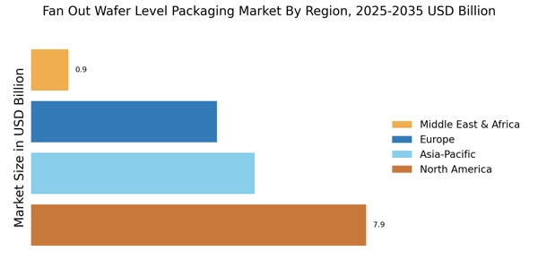
    North America : Technology Innovation Leader

    North America is the largest market for Fan Out Wafer Level Packaging (FOWLP), holding approximately 45% of the global market share. The region's growth is driven by the increasing demand for advanced semiconductor technologies, particularly in consumer electronics and automotive sectors. Regulatory support for innovation and investment in R&D further catalyzes market expansion, with initiatives aimed at enhancing semiconductor manufacturing capabilities. The competitive landscape in North America is robust, featuring key players such as Intel Corporation, Qualcomm Technologies, and Texas Instruments. These companies are at the forefront of technological advancements in FOWLP, leveraging their extensive R&D resources. The presence of leading universities and research institutions also fosters collaboration and innovation, ensuring that North America remains a pivotal hub for semiconductor packaging technologies.

    Europe : Emerging Semiconductor Hub

    Europe is witnessing significant growth in the Fan Out Wafer Level Packaging market, accounting for approximately 25% of the global share. The region's demand is fueled by the increasing adoption of IoT devices and automotive electronics, alongside supportive government policies aimed at bolstering semiconductor manufacturing. The European Union's initiatives to enhance technological sovereignty and reduce dependency on non-EU suppliers are pivotal in driving market growth. Leading countries in Europe include Germany, France, and the Netherlands, with a competitive landscape featuring companies like STMicroelectronics and NXP Semiconductors. The region is also home to various research institutions that collaborate with industry players to advance packaging technologies. This synergy between academia and industry is crucial for fostering innovation and maintaining Europe's competitive edge in the semiconductor sector.

    Asia-Pacific : Manufacturing Powerhouse

    Asia-Pacific is the second-largest market for Fan Out Wafer Level Packaging, holding around 30% of the global market share. The region's growth is primarily driven by the booming electronics manufacturing sector, particularly in countries like China, South Korea, and Taiwan. The increasing demand for high-performance chips in consumer electronics and telecommunications is a significant catalyst for market expansion, supported by favorable government policies promoting semiconductor production. China and Taiwan are leading countries in this market, with major players like Taiwan Semiconductor Manufacturing Company and Samsung Electronics dominating the landscape. The competitive environment is characterized by rapid technological advancements and significant investments in R&D. The presence of a well-established supply chain further enhances the region's capability to meet the growing demand for advanced packaging solutions.

    Middle East and Africa : Emerging Market Potential

    The Middle East and Africa (MEA) region is gradually emerging in the Fan Out Wafer Level Packaging market, currently holding about 5% of the global share. The growth is driven by increasing investments in technology and infrastructure, particularly in countries like the United Arab Emirates and South Africa. Government initiatives aimed at diversifying economies and promoting technology adoption are key factors contributing to market development in this region. While the competitive landscape is still developing, there is a growing interest from international players looking to establish a presence in the MEA market. Local companies are also beginning to invest in semiconductor technologies, creating opportunities for collaboration and innovation. As the region continues to invest in technology, the potential for growth in FOWLP is significant, paving the way for future advancements in semiconductor packaging.

    Key Players and Competitive Insights

    The Fan Out Wafer Level Packaging Market is currently characterized by a dynamic competitive landscape, driven by the increasing demand for advanced packaging solutions in consumer electronics, automotive, and telecommunications sectors. Key players such as Taiwan Semiconductor Manufacturing Company (TW), Samsung Electronics (KR), and Intel Corporation (US) are at the forefront, each adopting distinct strategies to enhance their market positioning. Taiwan Semiconductor Manufacturing Company (TW) focuses on innovation and technological advancements, particularly in developing high-density packaging solutions that cater to the growing needs of 5G and AI applications. Meanwhile, Samsung Electronics (KR) emphasizes regional expansion and strategic partnerships, aiming to bolster its manufacturing capabilities and supply chain resilience. Intel Corporation (US) is actively pursuing digital transformation initiatives, integrating AI and machine learning into its packaging processes to improve efficiency and reduce time-to-market.

    The business tactics employed by these companies reflect a concerted effort to localize manufacturing and optimize supply chains, which is crucial in a moderately fragmented market. The collective influence of these key players shapes a competitive structure that encourages innovation while also fostering collaboration among industry stakeholders. This environment is conducive to the emergence of new technologies and methodologies that enhance the overall efficiency of fan-out wafer level packaging.

    In August 2025, Taiwan Semiconductor Manufacturing Company (TW) announced a significant investment in a new facility dedicated to advanced packaging technologies. This strategic move is expected to enhance their production capacity and solidify their leadership position in the market, particularly in response to the surging demand for high-performance chips. The establishment of this facility not only underscores TSMC's commitment to innovation but also reflects a broader trend of companies investing in localized manufacturing to mitigate supply chain disruptions.

    In September 2025, Samsung Electronics (KR) entered into a partnership with a leading AI technology firm to develop next-generation packaging solutions that leverage artificial intelligence for enhanced performance. This collaboration is poised to revolutionize the packaging landscape by integrating smart technologies that optimize design and manufacturing processes. Such strategic alliances indicate a shift towards more sophisticated, technology-driven solutions that could redefine competitive advantages in the market.

    In October 2025, Intel Corporation (US) unveiled its latest packaging technology that incorporates advanced thermal management features, aimed at improving the performance of high-power computing applications. This innovation is particularly relevant as the demand for efficient thermal solutions continues to rise in the context of high-performance computing and data centers. Intel's focus on integrating cutting-edge technology into its packaging solutions illustrates a broader trend of prioritizing innovation over traditional price-based competition.

    As of October 2025, the competitive trends within the Fan Out Wafer Level Packaging Market are increasingly defined by digitalization, sustainability, and the integration of AI technologies. Strategic alliances are becoming more prevalent, as companies recognize the value of collaboration in driving innovation and enhancing supply chain reliability. Looking ahead, it appears that competitive differentiation will increasingly hinge on technological advancements and the ability to deliver sustainable, high-quality solutions, rather than merely competing on price. This shift suggests a transformative phase in the market, where innovation and reliability will be paramount.

    Key Companies in the Fan Out Wafer Level Packaging Market market include

    Industry Developments

    The Fan Out Wafer Level Packaging market is projected to reach USD 27.5 billion by 2032, exhibiting a CAGR of 6.66% during the forecast period (2024-2032). Key factors driving market growth include the increasing adoption of advanced packaging technologies, rising demand for miniaturization and integration, and growing applications in consumer electronics, communication infrastructure, and automotive sectors.

    Recent news developments include Amkor Technology's announcement of a new Fan Out Wafer Level Packaging facility in Japan and ASE Technology's collaboration with Qualcomm to develop advanced packaging solutions for 5G and AI applications.

    .webp

    Future Outlook

    Fan Out Wafer Level Packaging Market Future Outlook

    The Fan Out Wafer Level Packaging Market is projected to grow at a 6.66% CAGR from 2024 to 2035, driven by advancements in semiconductor technology and increasing demand for miniaturized electronics.

    New opportunities lie in:

    • Development of advanced thermal management solutions for high-performance applications.
    • Expansion into emerging markets with tailored packaging solutions.
    • Strategic partnerships with AI and IoT firms to enhance product integration.

    By 2035, the market is expected to solidify its position as a leader in innovative packaging solutions.

    Market Segmentation

    Fan Out Wafer Level Packaging Market Application Outlook

    • Smartphones
    • Tablets
    • Automotive
    • Wearables
    • Artificial Intelligence (AI) and Machine Learning (ML)

    Fan Out Wafer Level Packaging Market Product Type Outlook

    • Fan-Out Panel-Level Packaging (FOPLP)
    • Fan-Out in Laminate (FOIL)
    • Embedded Die Fan-Out Wafer Level Packaging (eDFOWLP)

    Fan Out Wafer Level Packaging Market Wafer Diameter Outlook

    • 200 mm
    • 300 mm

    Fan Out Wafer Level Packaging Market Substrate Material Outlook

    • Glass
    • Polymer
    • Interposer

    Report Scope

    MARKET SIZE 202417.52(USD Billion)
    MARKET SIZE 202518.69(USD Billion)
    MARKET SIZE 203535.62(USD Billion)
    COMPOUND ANNUAL GROWTH RATE (CAGR)6.66% (2024 - 2035)
    REPORT COVERAGERevenue Forecast, Competitive Landscape, Growth Factors, and Trends
    BASE YEAR2024
    Market Forecast Period2025 - 2035
    Historical Data2019 - 2024
    Market Forecast UnitsUSD Billion
    Key Companies ProfiledMarket analysis in progress
    Segments CoveredMarket segmentation analysis in progress
    Key Market OpportunitiesAdvancements in miniaturization and integration drive demand in the Fan Out Wafer Level Packaging Market.
    Key Market DynamicsTechnological advancements drive innovation in Fan Out Wafer Level Packaging, enhancing performance and reducing manufacturing costs.
    Countries CoveredNorth America, Europe, APAC, South America, MEA

    Leave a Comment

    FAQs

    What is the projected market valuation of the Fan Out Wafer Level Packaging Market by 2035?

    The projected market valuation for the Fan Out Wafer Level Packaging Market is expected to reach 35.62 USD Billion by 2035.

    What was the market valuation of the Fan Out Wafer Level Packaging Market in 2024?

    The overall market valuation of the Fan Out Wafer Level Packaging Market was 17.52 USD Billion in 2024.

    What is the expected CAGR for the Fan Out Wafer Level Packaging Market during the forecast period 2025 - 2035?

    The expected CAGR for the Fan Out Wafer Level Packaging Market during the forecast period 2025 - 2035 is 6.66%.

    Which companies are considered key players in the Fan Out Wafer Level Packaging Market?

    Key players in the Fan Out Wafer Level Packaging Market include Taiwan Semiconductor Manufacturing Company, Samsung Electronics, Intel Corporation, and others.

    What are the main product types in the Fan Out Wafer Level Packaging Market?

    The main product types in the Fan Out Wafer Level Packaging Market include Fan-Out Panel-Level Packaging, Fan-Out in Laminate, and Embedded Die Fan-Out Wafer Level Packaging.

    How does the market for 300 mm wafers compare to 200 mm wafers in terms of valuation?

    The market valuation for 300 mm wafers was 11.0 USD Billion in 2024, compared to 6.52 USD Billion for 200 mm wafers.

    What applications are driving growth in the Fan Out Wafer Level Packaging Market?

    Applications driving growth include smartphones, tablets, automotive, wearables, and artificial intelligence.

    What was the valuation of the Fan-Out Panel-Level Packaging segment in 2024?

    The valuation of the Fan-Out Panel-Level Packaging segment was 6.5 USD Billion in 2024.

    What substrate materials are utilized in the Fan Out Wafer Level Packaging Market?

    Substrate materials utilized include glass, polymer, and interposer, with interposer valued at 9.02 USD Billion in 2024.

    What is the projected growth for the automotive application segment in the Fan Out Wafer Level Packaging Market?

    The automotive application segment is projected to grow from 2.5 USD Billion in 2024 to 5.0 USD Billion by 2035.

    Download Free Sample

    Kindly complete the form below to receive a free sample of this Report

    Case Study
    Chemicals and Materials

    Compare Licence

    ×
    Features License Type
    Single User Multiuser License Enterprise User
    Price $4,950 $ $7,250
    Maximum User Access Limit 1 User Upto 10 Users Unrestricted Access Throughout the Organization
    Free Customization
    Direct Access to Analyst
    Deliverable Format
    Platform Access
    Discount on Next Purchase 10% 15% 15%
    Printable Versions