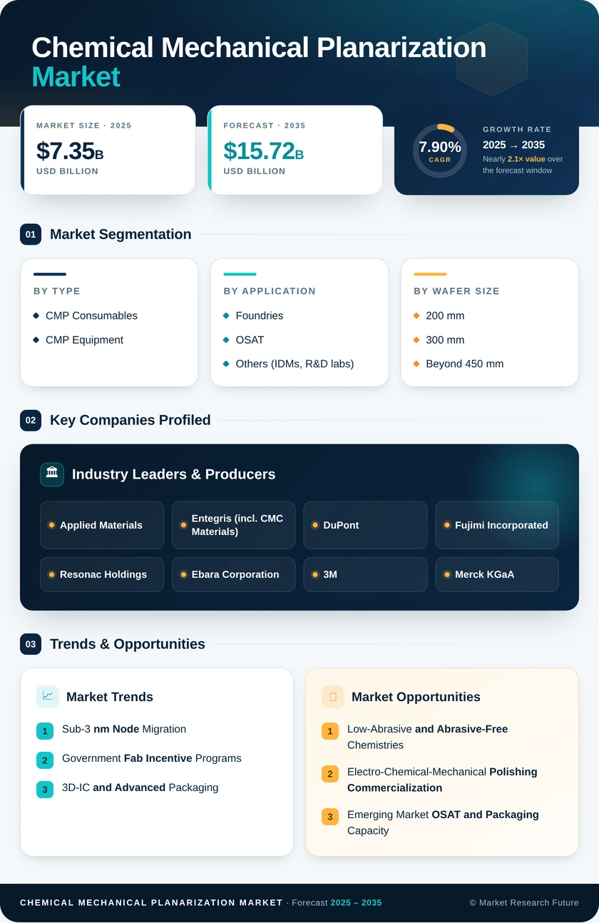
Segmentation Quick Reference
| Dimension | Sub-Segments | Dominant Segment | Fastest Growing Segment |
| Product Type | CMP Equipment; CMP Consumables | CMP Consumables | CMP Equipment |
| Application | Integrated Circuits; Compound Semiconductors; MEMS and NEMS; Advanced Packaging; Others | Integrated Circuits | Compound Semiconductors |
| End-User | Foundries; OSAT; Others (IDMs, R&D Labs) | Foundries | OSAT |
| Wafer Size | 200 mm; 300 mm; Beyond 450 mm | 300 mm | Beyond 450 mm |
| Geography | North America; Europe; Asia-Pacific; South America; Middle East & Africa | Asia-Pacific | South America |
Market Segmentation Overview
By Product Type
| Sub-Segment | Key Trend |
| CMP Consumables | Node-specific slurry formulations and multi-step polishing sequences drive recurring revenue growth |
| CMP Equipment | Greenfield fab investments in the United States, Europe, and Asia-Pacific fuel new tool installations |
CMP consumables represent the revenue backbone of the industry, with slurry and pad volumes tied directly to wafer start volumes across all process nodes. CMP equipment demand is lumpier, concentrated in fab construction cycles, but carries higher average selling prices per unit.
By Application
| Sub-Segment | Key Trend |
| Integrated Circuits | Leading-edge logic and memory node transitions increase planarization passes per wafer |
| Compound Semiconductors | SiC and GaN device scaling demands specialized abrasive and chemistry formulations |
| MEMS and NEMS | Automotive sensor proliferation and IoT device growth sustain mature-node CMP demand |
| Advanced Packaging | Hybrid bonding and TSV processes require ultra-flat surfaces with sub-nanometer roughness |
| Others | Optical components and photonics substrates represent niche but growing applications |
Integrated circuits and advanced packaging together account for the majority of CMP consumable consumption, while compound semiconductors offer the fastest growth trajectory due to the electric vehicle and renewable energy power electronics boom.
By End-User
| Sub-Segment | Key Trend |
| Foundries | Contract manufacturers at leading-edge nodes dominate global CMP tool and consumable procurement |
| OSAT | Advanced packaging ramp creates new CMP demand at outsourced assembly and test providers |
| Others (IDMs, R&D Labs) | Integrated device manufacturers maintain in-house CMP for proprietary process control |
Foundries set the pace for advanced CMP technology adoption, with leading-edge fabs qualifying new slurry and pad combinations 12–18 months ahead of volume production ramps. OSAT providers are emerging as a significant growth vector as chiplet architectures require planarization capabilities previously confined to front-end fabs.
By Wafer Size
| Sub-Segment | Key Trend |
| 200 mm | Sustained demand from analog, power, and specialty device manufacturing |
| 300 mm | Dominant wafer size for leading-edge logic, memory, and advanced packaging production |
| Beyond 450 mm | Long-term R&D stage; commercial viability dependent on industry consortium investment |
300 mm substrates will remain the industry standard throughout the forecast period, with 200 mm maintaining a stable, resilient niche. Beyond-450 mm wafer sizes remain in exploratory R&D, with meaningful commercial adoption unlikely before the early 2030s at the earliest.