Segmentation Quick Reference
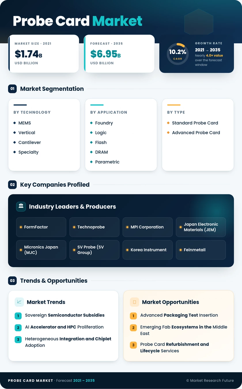
| Dimension | Sub-Segments | Dominant Segment | Fastest Growing Segment |
| Technology | MEMS, Vertical, Cantilever, Specialty | MEMS (~48% share, 2025) | Vertical (CAGR ~11.5%) |
| Application | Foundry and Logic, Flash, DRAM, Parametric | Foundry and Logic (~54% share, 2025) | Flash (CAGR ~11.9%) |
| Type | Standard Probe Card, Advanced Probe Card | Standard Probe Card (~56% share, 2025) | Advanced Probe Card (CAGR ~12.3%) |
| End User | Foundries, IDMs, OSATs, Research Institutes | Foundries (~60% share, 2025) | OSATs (CAGR ~13.2%) |
| Wafer Size | Up to 150 mm, 200 mm, 300 mm, 450 mm | 300 mm (~66% share, 2025) | 450 mm (CAGR ~14.5%) |
Market Segmentation Overview
By Technology
| Sub-Segment | Key Trend |
| MEMS | Dominant architecture for advanced nodes; highest installed base across logic and memory fabs |
| Vertical | Fastest-growing MEMS variant; preferred for HBM, AI accelerators, and sub-3 nm probing |
| Cantilever | Declining share but retains relevance in mature-node parametric and analog testing |
| Specialty | Niche growth in RF, photonics, and wide-bandgap device verification |
MEMS technology continues to set the standard for high-density wafer probing across the semiconductor industry. Vertical variants are capturing the performance-critical segments where pin counts exceed 50,000 per card and positional accuracy must remain within single-micrometer tolerances.
By Application
| Sub-Segment | Key Trend |
| Foundry and Logic | Largest category driven by contract foundry volume and continuous node migration |
| Flash | Fastest growth; 200+ layer 3D NAND architecture expansion drives test complexity |
| DRAM | HBM3E and DDR5 production ramps are elevating multi-die probe requirements |
| Parametric | Steady demand linked to process control and yield optimization workflows |
Foundry and logic testing absorbs the largest share of probe card spending as leading foundries operate across multiple technology nodes simultaneously. Flash memory testing is growing fastest as each new 3D NAND generation increases die complexity and expands the probe card touchdown footprint.
By Type
| Sub-Segment | Key Trend |
| Standard Probe Card | Majority of unit shipments; cost-optimized for high-volume mature-node production |
| Advanced Probe Card | Rapidly growing; engineered for high-frequency, high-pin-count AI and HPC testing |
Standard probe cards serve the volume market, while advanced designs address the performance frontier. The advanced segment is growing at nearly double the overall rate as AI chip complexity and chiplet architectures demand specialized test solutions.
By End User
| Sub-Segment | Key Trend |
| Foundries | Largest spender; dominates procurement through long-term supply agreements |
| IDMs | Steady growth driven by vertical integration in automotive and analog segments |
| OSATs | Fastest-growing buyer segment; chiplet assembly migration creating new test budgets |
| Research Institutes | Smallest segment; focused on next-generation material and device R&D |
Foundries remain the dominant end-user category by spending share, reflecting the outsourced manufacturing model's grip on global wafer production. OSATs represent the most dynamic growth pocket as wafer-level test responsibility shifts toward assembly and test houses.
By Wafer Size
| Sub-Segment | Key Trend |
| Up to 150 mm | Specialty applications in analog, MEMS sensors, and compound semiconductors |
| 200 mm | Resilient demand from automotive, IoT, and power device production |
| 300 mm | Dominant wafer size for leading-edge logic and memory fabrication |
| 450 mm | Pilot-stage development; potential volume adoption in the early 2030s |
The 300 mm wafer size dominates the probe card landscape, reflecting its status as the industry standard for advanced logic and memory production. Growth in 200 mm is sustained by automotive and power semiconductor demand, while 450 mm remains in pilot stage with potential to emerge as a cost-reduction lever for high-volume logic manufacturers.