Semiconductor Inspection System Market

반도체 검사 시스템 시장 규모, 점유율 및 연구 보고서 유형별(웨이퍼 및 마스크), 최종 사용자별(SME 및 대기업), 지역별(북미, 유럽, 아시아 태평양 및 기타 지역) – 산업 규모, 점유율 및 2035년까지의 성장
ID: MRFR/SEM/1265-CR 110 Pages Ankit Gupta Last Updated: September 29, 2026
Semiconductor Inspection System Market
Market Size
Forecast Period2025 - 2035
CAGR (2025 - 2035)4.45%
2024 Market Size$ 6.4 Billion
2025 Market Size$ 6.68 Billion
2035 Market Size$ 10.33 Billion
Key Players
ASML
KLA Corporation
Applied Materials
Nikon Corporation
Hitachi High-Technologies Corporation
Teradyne
Opportunities
  • Growing Focus on Quality Assurance
  • Regulatory Compliance and Industry Standards
  • Increasing Complexity of Semiconductor Devices

Semiconductor Inspection System Market 요약

주요 시장 동향 및 하이라이트

시장 규모 및 예측

CAGR (2025 - 2035) 4.45%

주요 기업

ASML (NL), KLA Corporation (US), Applied Materials (US), Nikon Corporation (JP), Hitachi High-Technologies Corporation (JP), Teradyne (US), Rudolph Technologies (US), Cohu (US)

Semiconductor Inspection System Market Treiber

Growing Focus on Quality Assurance

Regulatory Compliance and Industry Standards

Increasing Complexity of Semiconductor Devices

The increasing complexity of semiconductor devices is a critical driver for the Semiconductor Inspection System Market. As semiconductor technology evolves, devices are becoming more intricate, with smaller geometries and more layers. This complexity necessitates advanced inspection systems capable of identifying defects that could compromise device performance. Manufacturers are investing in state-of-the-art inspection technologies to address these challenges, ensuring that they can deliver high-quality products. The market for semiconductor inspection systems is expected to expand as companies seek to enhance their production capabilities and maintain compliance with industry standards. This trend highlights the importance of robust inspection processes in the semiconductor manufacturing landscape.

Rising Demand for High-Performance Electronics

Technological Advancements in Inspection Systems

시장 세그먼트 통찰력

유형별: 웨이퍼(가장 큰) 대 마스크(가장 빠르게 성장하는)

반도체 검사 시스템 시장에서 웨이퍼는 통합 회로 및 마이크로 전자 제품 제조에 광범위하게 사용되기 때문에 시장의 상당 부분을 차지하는 가장 큰 세그먼트를 나타냅니다. 이 세그먼트의 지배력은 웨이퍼 가공을 위한 고정밀 검사 시스템이 필요한 고급 반도체 장치에 대한 수요 증가에 의해 주로 촉진됩니다. 반대로, 마스크 세그먼트는 더 작지만 빠르게 주목받고 있으며 시장 내에서 가장 빠르게 성장하는 범주로 인식되고 있습니다. 이 성장은 반도체 제조에서 포토리소그래피 공정의 중요성이 증가하고 있음을 반영하며, 마스크 품질은 반도체 장치의 성능에 직접적인 영향을 미칩니다.

웨이퍼(지배적) 대 마스크(신흥)

웨이퍼는 반도체 검사 시스템 시장에서 지배적인 세그먼트로 간주되며, 반도체 생산에서 중요한 역할을 합니다. 그 중요성은 통합 회로가 요구되는 사양과 품질에 맞게 제작되도록 보장하는 데 필요하기 때문에 발생하며, 이는 실패한 장치로 이어질 수 있는 결함을 방지합니다. 반면, 마스크 세그먼트는 이 시장의 신흥 측면을 나타내며, 포토리소그래피의 기술 발전에 의해 촉발된 수요 급증을 경험하고 있습니다. 반도체 설계의 복잡성이 증가함에 따라, 고도로 정확하고 결함이 없는 마스크에 대한 필요성이 중요해졌으며, 이는 마스크 응용 프로그램에 맞춘 검사 시스템의 혁신을 촉진하고 있습니다. 이 두 세그먼트 간의 상호작용은 반도체 제조의 진화하는 환경을 강조합니다.

최종 사용자별: 대기업(가장 큰) 대 중소기업(SME)(가장 빠르게 성장하는)

반도체 검사 시스템 시장에서 시장 점유율의 분포는 대기업 쪽으로 뚜렷하게 기울어져 있으며, 이들은 상당한 자원과 확립된 시장 존재로 인해 상당한 부분을 차지하고 있습니다. 이 세그먼트는 고급 반도체 검사 기술에 대한 투자를 가능하게 하는 광범위한 재정적 능력으로 혜택을 보고 있으며, 고품질 생산을 보장합니다. 반면, 중소기업(SME)은 더 유연한 운영 요구에 맞는 정밀 검사 시스템의 필요성에 의해 주목받고 있으며, 이는 시장 환경의 역동적인 변화를 나타냅니다.

최종 사용자: 대기업(지배적) 대 중소기업(SME)(신흥)

대기업은 규모, 운영 능력 및 최신 검사 기술에 투자할 수 있는 능력 덕분에 반도체 검사 시스템 시장을 지배하고 있습니다. 이들은 종종 혁신의 최전선에 있으며, 품질 관리 프로세스를 향상시키기 위해 정교한 시스템을 통합하여 산업 표준 준수를 보장합니다. 반대로, 중소기업(SME)은 유연하고 비용 효율적인 검사 솔루션을 채택함으로써 중요한 플레이어로 부상하고 있습니다. 이들은 규모보다 적응성과 효율성을 우선시하는 경향이 있으며, 전문화된 검사 응용 프로그램이 필요한 틈새 시장에서 중요한 발전을 이루어 이 세그먼트의 성장을 촉진하고 있습니다.

Semiconductor Inspection System Market에 대한 더 자세한 통찰력 얻기

지역 통찰력

North America : Innovation and Leadership Hub

North America is the largest market for semiconductor inspection systems, holding approximately 45% of the global market share. The region's growth is driven by robust demand for advanced semiconductor technologies, fueled by increasing investments in AI, IoT, and automotive sectors. Regulatory support for technology innovation and manufacturing incentives further catalyze market expansion. The United States leads the market, with key players like KLA Corporation, Applied Materials, and Teradyne headquartered here. The competitive landscape is characterized by continuous innovation and strategic partnerships among these companies, ensuring a strong foothold in the global market. The presence of advanced research institutions also bolsters the region's capabilities in semiconductor inspection technologies.

Europe : Emerging Semiconductor Powerhouse

Europe is witnessing significant growth in the semiconductor inspection system market, accounting for around 25% of the global share. The region benefits from strong governmental support for semiconductor initiatives, particularly in countries like Germany and France, which are investing heavily in local manufacturing and R&D. Regulatory frameworks aimed at enhancing technological capabilities are also pivotal in driving market demand. Germany stands out as a leader in the market, with major players like ASML and Nikon Corporation establishing a strong presence. The competitive landscape is evolving, with European companies focusing on innovation and sustainability to meet the growing demand for advanced semiconductor technologies. Collaborative efforts among industry stakeholders are also enhancing the region's market position.

Asia-Pacific : Rapid Growth and Expansion

Asia-Pacific is a rapidly growing market for semiconductor inspection systems, holding approximately 20% of the global market share. The region's growth is primarily driven by the increasing demand for consumer electronics and automotive applications, particularly in countries like China, Japan, and South Korea. Government initiatives aimed at boosting semiconductor manufacturing capabilities are also significant growth catalysts. China is the largest market in the region, with substantial investments in semiconductor technology and manufacturing. The competitive landscape features key players like Hitachi High-Technologies and Nikon Corporation, which are focusing on innovation to meet the rising demand. The presence of a robust supply chain and skilled workforce further enhances the region's competitiveness in the semiconductor inspection market.

Middle East and Africa : Emerging Market Potential

The Middle East and Africa region is gradually emerging in the semiconductor inspection system market, currently holding about 10% of the global share. The growth is driven by increasing investments in technology and infrastructure, particularly in countries like Israel and South Africa. Government initiatives aimed at fostering innovation and attracting foreign investments are also contributing to market expansion. Israel is a key player in the region, with a focus on advanced semiconductor technologies. The competitive landscape is characterized by a mix of local and international companies, with a growing emphasis on research and development. As the region continues to invest in technology, the semiconductor inspection market is expected to see significant growth in the coming years.
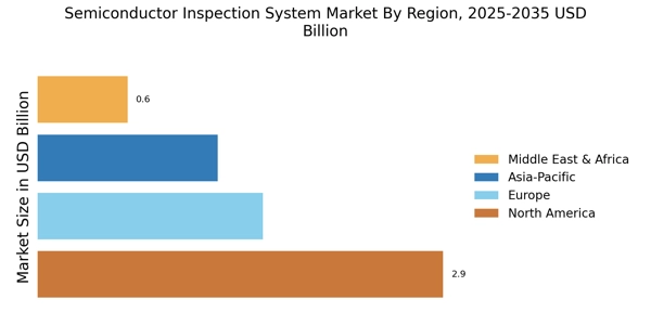
Semiconductor Inspection System Market Regional Image

주요 기업 및 경쟁 통찰력

주요 시장 기업들은 제품 라인을 늘리기 위해 R&D에 광범위하게 투자하고 있으며, 이는 반도체 검사 시스템 시장의 성장을 더욱 촉진할 것입니다. 중요한 시장 발전에는 신제품 출시, 계약 체결, 인수 및 합병, 더 큰 투자, 그리고 다른 조직과의 협력이 포함됩니다. 반도체 검사 시스템 산업은 경쟁이 치열하고 증가하는 시장 환경에서 번창하고 성장하기 위해 비용 효율적인 상품을 생산해야 합니다. 운영 비용을 줄이기 위해 현지에서 제조하는 것은 전 세계 반도체 검사 시스템 산업에서 고객에게 서비스를 제공하고 시장 부문을 확장하기 위해 제조업체들이 사용하는 효과적인 비즈니스 전략입니다. 반도체 검사 시스템 산업은 최근 몇 가지 중요한 혜택을 제공했습니다. KLA Corporation, Kraft Wafers Group Inc. 및 반도체 검사 시스템 시장의 다른 주요 경쟁자들은 연구 및 개발 활동에 투자하여 소비자 수요를 증가시키려 하고 있습니다. KLA Corporation은 캘리포니아 밀피타스에 본사를 둔 자본 장비 회사입니다. 이 회사는 반도체 및 기타 관련 나노전자 비즈니스에 프로세스 제어 및 수율 관리 기술을 제공합니다. 연구 및 개발에서 최종 대량 생산에 이르기까지 회사의 제품과 서비스는 웨이퍼, 레티클, 집적 회로(IC), 패키지 생산의 모든 단계에 초점을 맞추고 있습니다. 이들은 글로벌 리더의 규모와 나노미터 규모의 트랜지스터에서 마이크론 수준의 다이 상호 연결, 웨이퍼 및 패키지의 매크로 결함 검사, 금속 상호 연결 조성, 공장 분석 및 고급 반도체 패키징을 위한 리소그래피와 같은 최첨단 기술의 더 넓은 포트폴리오를 결합합니다. 이 범위의 폭은 고객과 협력하여 벌거벗은 실리콘 웨이퍼에서 최종 후면 패키징에 이르기까지 프로세스 수율 및 프로세스 수정에 대해 협력할 수 있게 합니다. Onto Innovation의 소프트웨어는 고객이 다양한 작업이 전체 제품에 미치는 영향을 더 잘 이해할 수 있도록 하여 제품 품질과 신뢰성을 향상시킬 수 있도록 합니다.
2023년 12월 KLA Corporation은 고급 메모리 칩 제조업체를 위한 새로운 Axion T2000 X-ray 계측 장비를 출시했습니다. Axion T2000은 이전에 들을 수 없었던 수준의 해상도, 정확성, 정밀도 및 속도로 높은 비율의 장치 특성을 측정하는 특허 기술을 사용합니다. 반도체 가치 사슬 전반에 걸쳐 독특한 통찰력을 가진 Onto Innovation은 프로세스 제어에서 독보적입니다. 그들은 고객이 가장 어려운 수율, 장치 성능, 품질 및 신뢰성 문제를 해결하도록 돕습니다. 소비자를 더 똑똑하고 빠르며 효율적으로 만들어 Onto Innovation은 그들의 중요한 발전 경로를 최적화할 것입니다. Onto Innovation은 매사추세츠주 윌밍턴에 본사를 두고 있으며 고객에게 글로벌 판매 및 서비스 조직을 제공합니다.
2024년 6월 Onto Innovation Inc.는 상위 3개 반도체 제조업체로서 새로운 EB40 모듈이 장착된 Dragonfly G3 시스템을 확보했습니다. 이 시스템과 모듈은 웨이퍼 엣지 및 뒷면의 결함으로 인한 수율 손실을 해결하기 위해 모든 표면 웨이퍼 검사를 제공합니다.

Semiconductor Inspection System Market 시장의 주요 기업은 다음과 같습니다

Recent Industry Developments

  • Q3 2026: Applied Materials (US): Announced Advantest as an Innovation Partner for its EPIC Center in Silicon Valley, co-locating an Advantest Innovation Center to bridge front-end manufacturing with back-end testing and improve integration of in-line metrology and inspection for AI and 3D advanced packaging.

  • Q3 2026: Hitachi High-Tech (JP): Launched sales and support activities in India for the FineSAT III ultrasonic inspection system, a non-destructive tool for detecting delamination, voids, and bonding failures in semiconductor packages, supporting quality assurance in India's expanding fab and OSAT ecosystem.

  • Q3 2026: Teradyne (US): Launched three new UltraFLEXplus instruments including the UltraPort-PCIe6, the industry's first high-speed I/O protocol ATE solution for PCIe Gen6 interfaces, enabling test coverage shifts to earlier insertions for improved Known Good Die confidence.

  • Q2 2024: Nikon Launches New NSR-2205iL1 Semiconductor Lithography System Nikon announced the launch of its new NSR-2205iL1 i-line stepper, designed for advanced semiconductor manufacturing and inspection, enhancing productivity and precision for chipmakers.
  • Q2 2024: KLA Introduces Next-Generation eBeam Inspection System for Advanced Nodes KLA unveiled a new eBeam inspection system targeting sub-5nm semiconductor nodes, offering improved defect detection and process control for leading-edge chip production.
  • Q2 2024: Applied Materials Expands Inspection Portfolio with New Optical Inspection Tool Applied Materials launched a new optical inspection tool aimed at accelerating defect detection in advanced semiconductor manufacturing, supporting the industry's move to smaller geometries.
  • Q2 2024: ASML Opens New Semiconductor Equipment Facility in South Korea ASML inaugurated a new facility in South Korea to support the growing demand for semiconductor inspection and lithography systems in the Asia-Pacific region.
  • Q3 2024: Nanotronics Secures $50 Million Series C Funding to Advance AI-Driven Inspection Systems Nanotronics raised $50 million in Series C funding to accelerate the development and deployment of its AI-powered semiconductor inspection platforms.
  • Q3 2024: KLA Announces Strategic Partnership with Samsung for Advanced Wafer Inspection KLA entered into a strategic partnership with Samsung Electronics to provide advanced wafer inspection systems for next-generation semiconductor manufacturing lines.
  • Q3 2024: Tokyo Electron Unveils New Defect Inspection System for 3D NAND Production Tokyo Electron introduced a new defect inspection system specifically designed for high-volume 3D NAND flash memory manufacturing, improving yield and process efficiency.
  • Q4 2024: Onto Innovation Launches Atlas 10 Metrology and Inspection Platform Onto Innovation launched the Atlas 10 platform, a new metrology and inspection system for advanced semiconductor packaging and heterogeneous integration.
  • Q4 2024: Camtek Receives Multi-System Order for Advanced Packaging Inspection from Leading OSAT Camtek announced a multi-system order from a leading outsourced semiconductor assembly and test (OSAT) provider for its advanced packaging inspection systems.
  • Q1 2025: KLA Appoints New Chief Technology Officer KLA announced the appointment of a new Chief Technology Officer to lead innovation in semiconductor inspection and metrology solutions.
  • Q1 2025: Applied Materials Wins Major Contract for Inspection Systems from Leading Foundry Applied Materials secured a significant contract to supply advanced inspection systems to a top global semiconductor foundry, supporting next-generation chip production.
  • Q2 2025: ASML Announces Expansion of R&D Center for Inspection Technologies in the Netherlands ASML announced the expansion of its R&D center in the Netherlands, focusing on the development of next-generation semiconductor inspection technologies.

향후 전망

Semiconductor Inspection System Market 향후 전망

반도체 검사 시스템 시장은 2025년부터 2035년까지 4.45%의 CAGR로 성장할 것으로 예상되며, 이는 기술 발전, 소형화에 대한 증가하는 수요 및 엄격한 품질 관리 요구에 의해 추진됩니다.

2035년까지 시장은 강력한 성장을 달성할 것으로 예상되며, 반도체 제조의 중요한 구성 요소로 자리 잡을 것입니다.

시장 세분화

반도체 검사 시스템 시장 유형 전망

  • 웨이퍼
  • 마스크

반도체 검사 시스템 시장 최종 사용자 전망

  • 중소기업
  • 대기업

보고서 범위

시장 규모 2024 64억 1천만 달러
시장 규모 2025 66억 8천5백만 달러
시장 규모 2035 103억 3천만 달러
연평균 성장률 (CAGR) 4.45% (2025 - 2035)
보고서 범위 수익 예측, 경쟁 환경, 성장 요인 및 동향
기준 연도 2024
시장 예측 기간 2025 - 2035
역사적 데이터 2019 - 2024
시장 예측 단위 억 달러
주요 기업 프로필 ASML (NL), KLA Corporation (US), Applied Materials (US), Nikon Corporation (JP), Hitachi High-Technologies Corporation (JP), Teradyne (US), Rudolph Technologies (US), Cohu (US)
다루는 세그먼트 유형, 최종 사용자, 지역
주요 시장 기회 인공지능의 발전이 반도체 검사 시스템 시장의 정밀도를 향상시킵니다.
주요 시장 역학 기술 발전이 진화하는 산업 표준 및 경쟁 압력 속에서 정교한 반도체 검사 시스템에 대한 수요를 이끌고 있습니다.
다루는 국가 북미, 유럽, 아시아 태평양, 남미, 중동 및 아프리카

Frequently Asked Questions

반도체 검사 시스템 시장의 현재 가치는 얼마입니까?

2024년 현재 시장 가치는 64.01억 달러입니다.

2035년까지 반도체 검사 시스템 시장의 예상 시장 규모는 얼마입니까?

2035년까지 시장 가치는 103.3억 달러에 이를 것으로 예상됩니다.

2025년부터 2035년까지 반도체 검사 시스템 시장의 예상 CAGR은 얼마입니까?

2025년부터 2035년까지 시장은 4.45%의 CAGR로 성장할 것으로 예상됩니다.

반도체 검사 시스템 시장의 주요 기업은 어디입니까?

주요 기업으로는 ASML, KLA Corporation, Applied Materials, Nikon Corporation, Hitachi High-Technologies Corporation, Teradyne, Rudolph Technologies, Cohu가 있습니다.

반도체 검사 시스템 시장의 시장 세그먼트는 무엇입니까?

시장 세그먼트에는 웨이퍼와 마스크가 포함되며, 각각의 예상 가치는 51.2억 달러와 52.1억 달러입니다.

반도체 검사 시스템 시장에서 중소기업(SME)은 대기업과 어떻게 비교됩니까?

2024년 중소기업은 19.2억 달러를 차지했으며, 대기업은 44.8억 달러의 시장 가치를 나타냈습니다.

2035년까지 반도체 검사 시스템 시장에서 중소기업의 예상 성장률은 얼마입니까?
중소기업은 2035년까지 30.5억 달러로 성장할 것으로 예상됩니다.
2035년까지 반도체 검사 시스템 시장에서 대기업의 예상 시장 성과는 어떻습니까?
대기업은 2035년까지 72.8억 달러의 가치를 달성할 것으로 예상됩니다.
반도체 검사 시스템 시장의 성장률은 다른 기술 분야와 어떻게 비교됩니까?
반도체 검사 시스템 시장의 성장은 견조해 보이며, 2025년부터 2035년까지 4.45%의 CAGR이 예상됩니다.
반도체 검사 시스템 시장의 성장을 이끄는 요인은 무엇입니까?
성장은 반도체 기술의 발전과 고품질 검사 시스템에 대한 수요 증가에 의해 촉진될 수 있습니다.
저자
Author Author Profile Ankit Gupta LinkedIn Team Lead - Research
Ankit Gupta is a seasoned market intelligence and strategic research professional with over six plus years of experience in the ICT and Semiconductor industries. With academic roots in Telecom, Marketing, and Electronics, he blends technical insight with business strategy. Ankit has led 200+ projects, including work for Fortune 500 clients like Microsoft and Rio Tinto, covering market sizing, tech forecasting, and go-to-market strategies. Known for bridging engineering and enterprise decision-making, his insights support growth, innovation, and investment planning across diverse technology markets.
무료 샘플 다운로드

이 보고서의 무료 샘플을 받으려면 아래 양식을 작성하십시오

Download PDF ×

We do not share your information with anyone. However, we may send you emails based on your report interest from time to time. You may contact us at any time to opt-out.